Increase (boost) a low voltage from a battery or other source to a stable 3.3V output with the XCL105B331H2-G and STM32F091RC
Synchronous step-up DC/DC converter with integrated switching FETs

Published Jun 04, 2024
Click board™
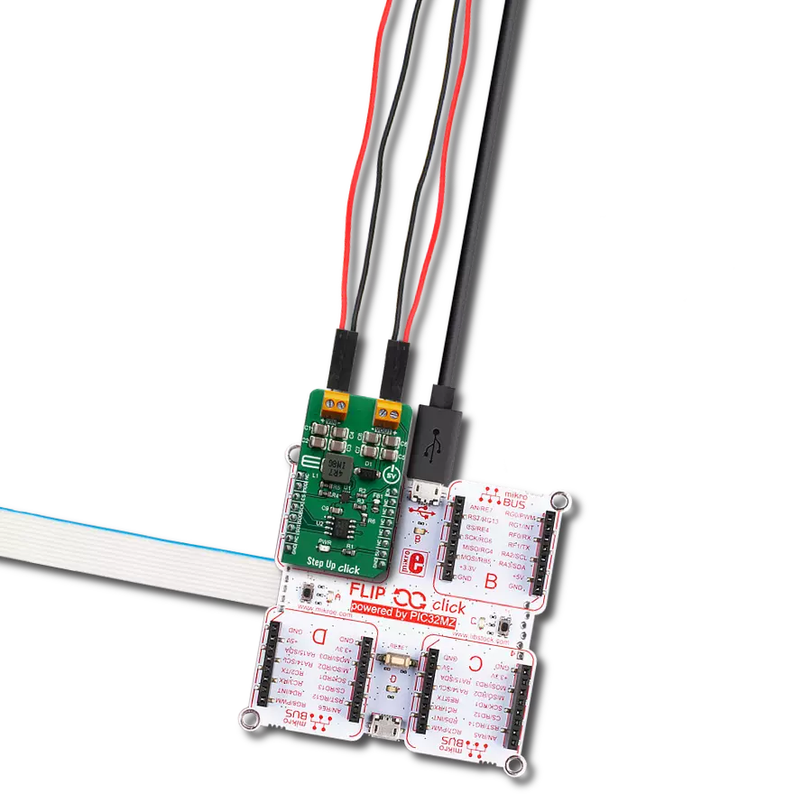
Boost 11 Click
Dev. board
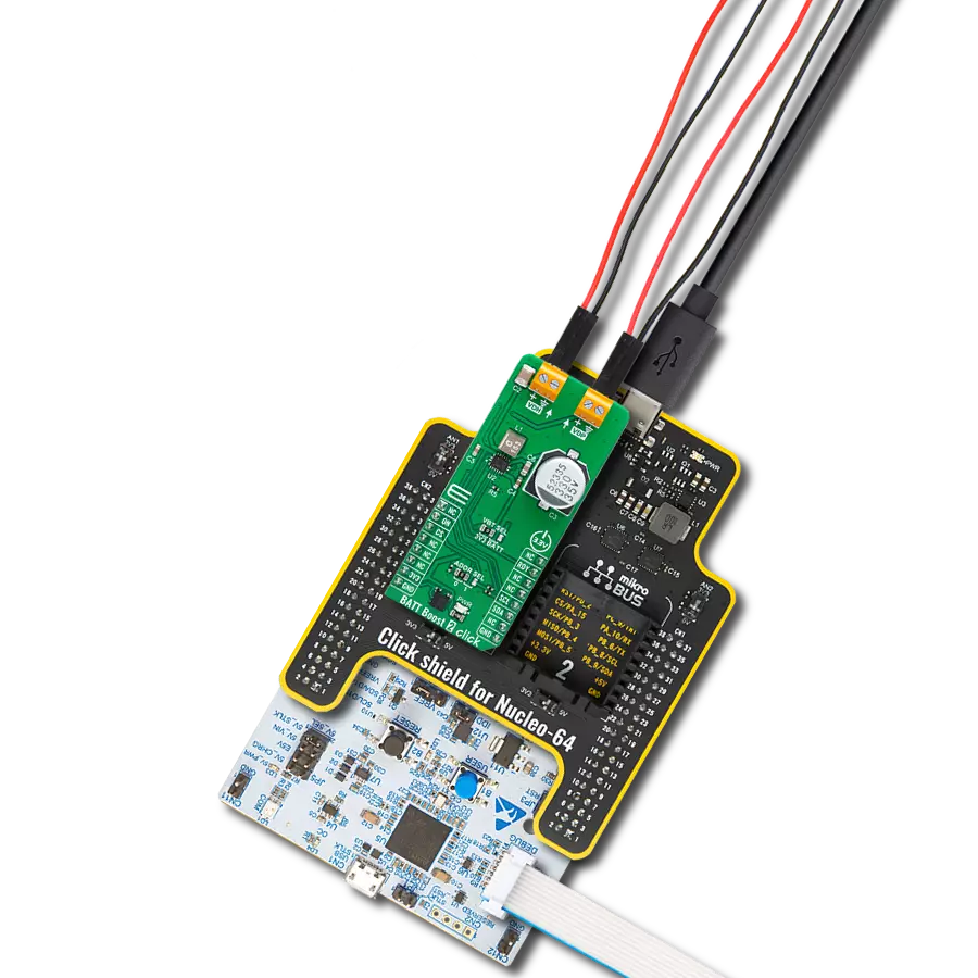
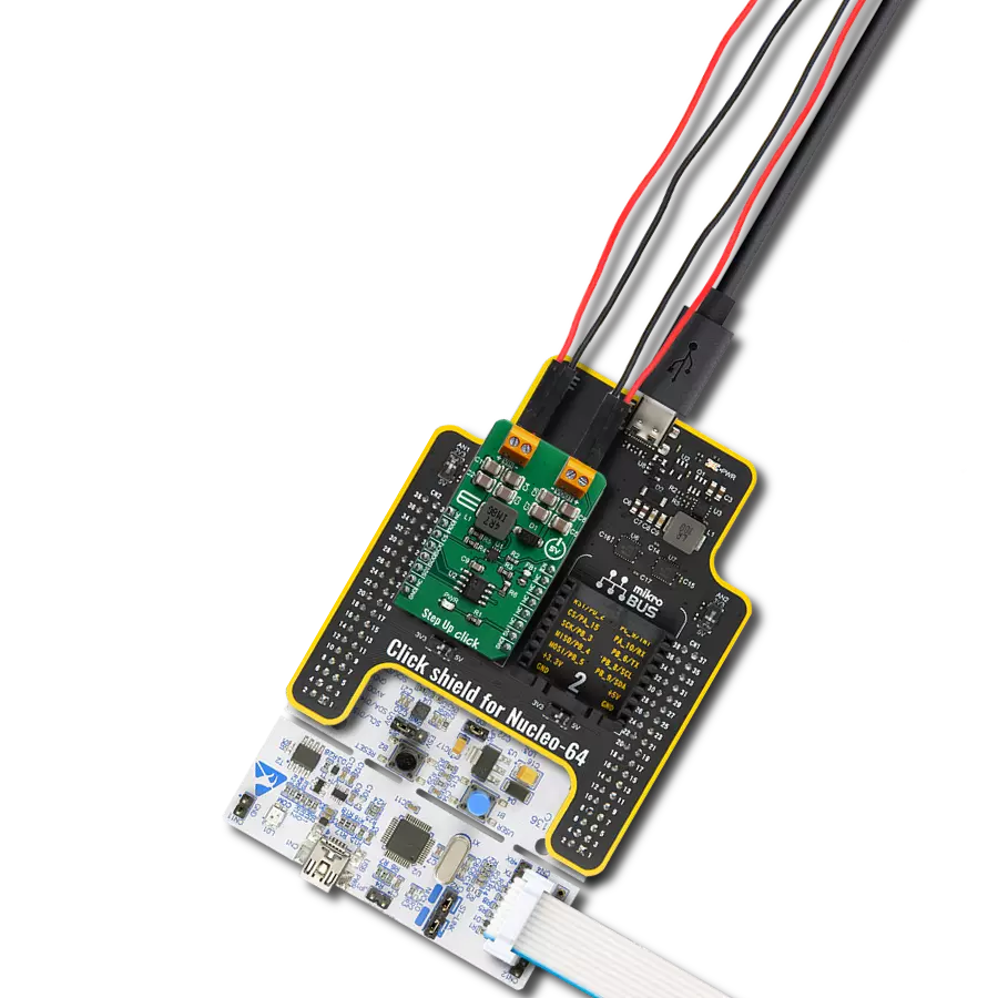
Nucleo-64 with STM32F091RC MCU
Compiler
NECTO Studio
MCU
STM32F091RC
Provide a reliable voltage boost for powering low-power sensors or other industrial electronics from low-voltage sources
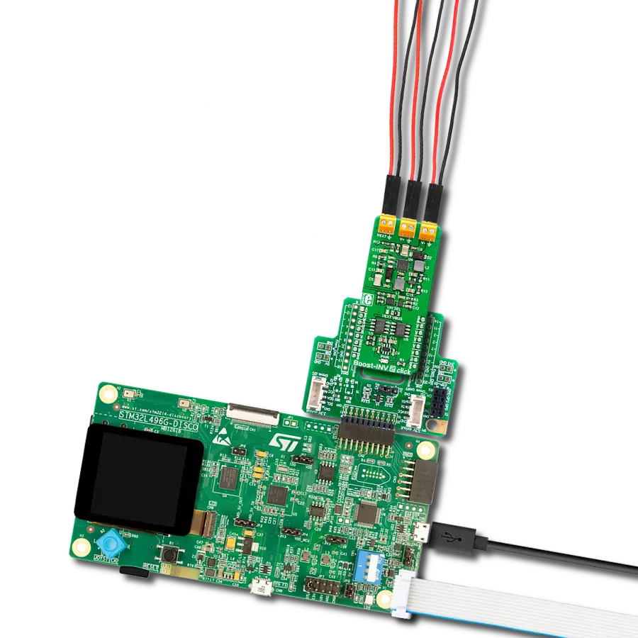
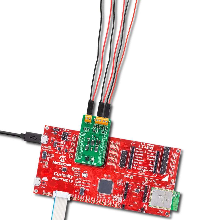
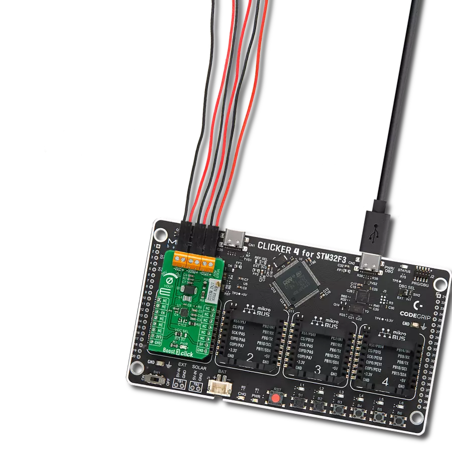
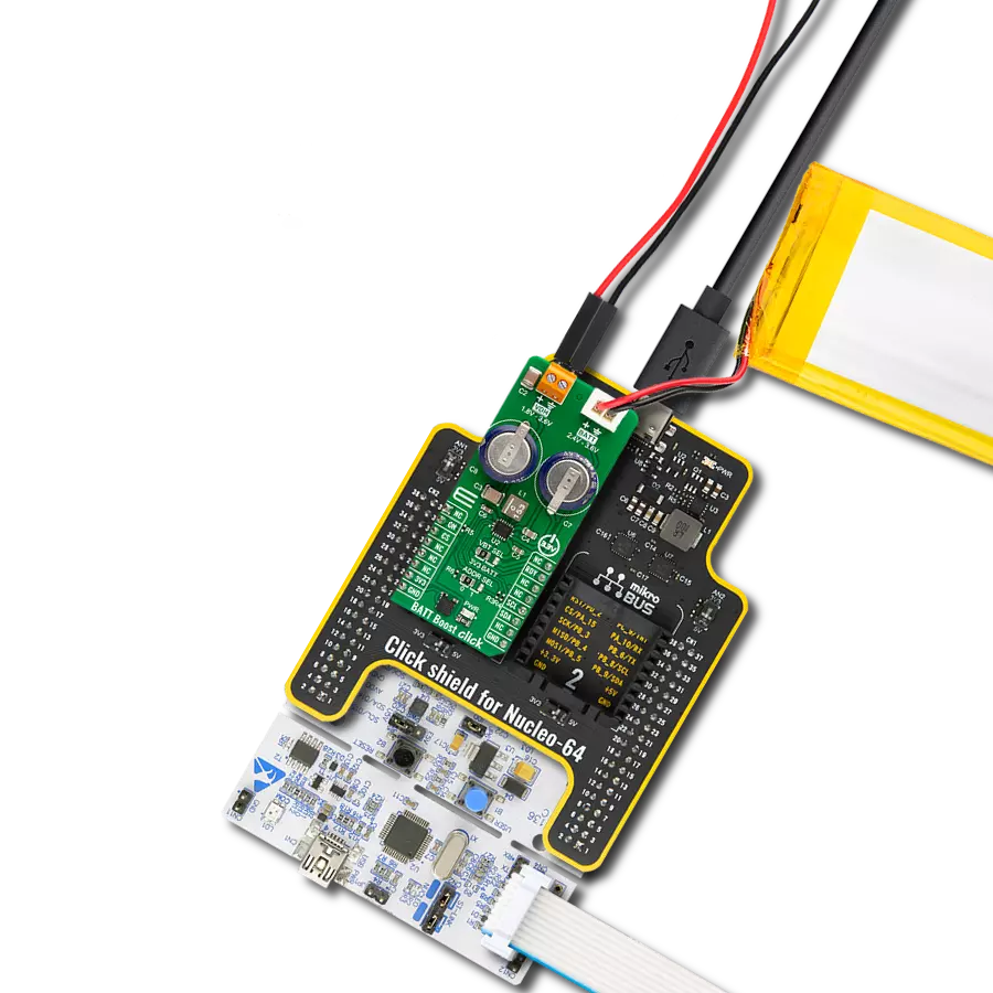
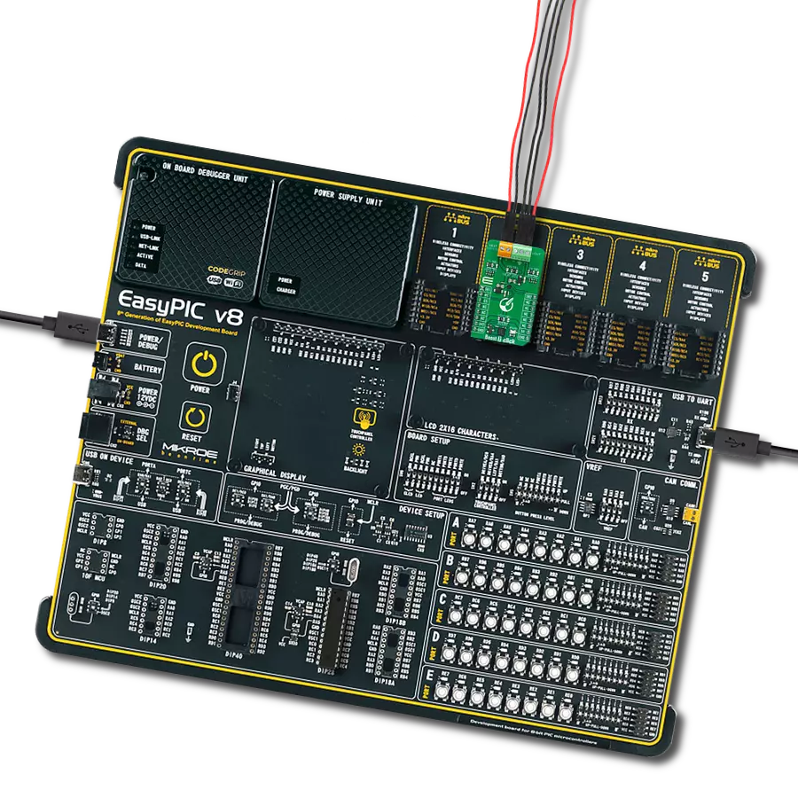
A
A
Hardware Overview
How does it work?
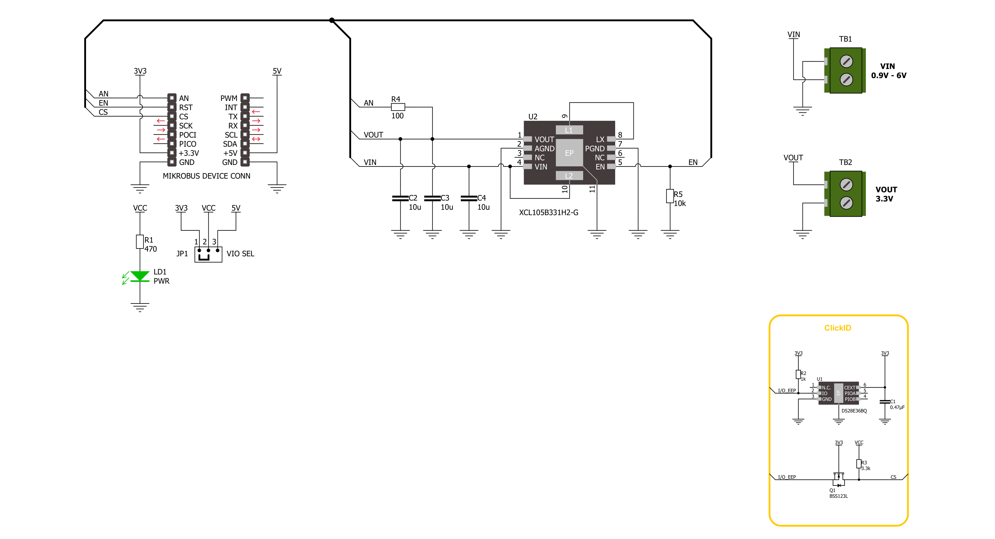
Boost 11 Click is based on the XCL105B331H2-G, a synchronous step-up DC/DC converter from TOREX Semi. This component includes a reference voltage source, ramp wave circuit, error amplifier, PWM comparator, phase compensation circuit, N-channel driver FET, P-channel synchronous switching FET, and current limiter circuit. It can start operating from an input voltage of 0.9V, making it suitable for devices using single Alkaline or Nickel-metal hydride batteries. The operating voltage range spans from 0.9V to 6V, which applies to the VIN terminal. This versatility makes it ideal for industrial equipment, Internet of Things (IoT) devices, wearables, and any applications
prioritizing battery life. The XCL105B331H2-G operates by using the error amplifier to compare the internal reference voltage with the feedback voltage. The resulting output undergoes phase compensation and is fed to the PWM comparator. This comparator matches the signal from the error amplifier with the ramp wave circuit output, sending the resulting signal to the buffer driver circuit to control the PWM duty cycle. This continuous process stabilizes the output voltage, fixed at 3.3V and available at the VOUT terminal. Additionally, an output signal is available on the AN pin of the mikroBUS™ socket. The Boost 11 Click uses the EN pin of the mikroBUS™ socket in addition to the
AN pin. When the EN pin is set to a high logic level, the output voltage is raised via the Start-Up mode, initiating normal operation. When set to a low logic level, the IC enters Standby mode, significantly reducing current consumption. This Click board™ can operate with either 3.3V or 5V logic voltage levels selected via the VIO SEL jumper. This way, both 3.3V and 5V capable MCUs can use the communication lines properly. Also, this Click board™ comes equipped with a library containing easy-to-use functions and an example code that can be used as a reference for further development.

Features overview
Development board
Nucleo-64 with STM32F091RC MCU offers a cost-effective and adaptable platform for developers to explore new ideas and prototype their designs. This board harnesses the versatility of the STM32 microcontroller, enabling users to select the optimal balance of performance and power consumption for their projects. It accommodates the STM32 microcontroller in the LQFP64 package and includes essential components such as a user LED, which doubles as an ARDUINO® signal, alongside user and reset push-buttons, and a 32.768kHz crystal oscillator for precise timing operations. Designed with expansion and flexibility in mind, the Nucleo-64 board features an ARDUINO® Uno V3 expansion connector and ST morpho extension pin
headers, granting complete access to the STM32's I/Os for comprehensive project integration. Power supply options are adaptable, supporting ST-LINK USB VBUS or external power sources, ensuring adaptability in various development environments. The board also has an on-board ST-LINK debugger/programmer with USB re-enumeration capability, simplifying the programming and debugging process. Moreover, the board is designed to simplify advanced development with its external SMPS for efficient Vcore logic supply, support for USB Device full speed or USB SNK/UFP full speed, and built-in cryptographic features, enhancing both the power efficiency and security of projects. Additional connectivity is
provided through dedicated connectors for external SMPS experimentation, a USB connector for the ST-LINK, and a MIPI® debug connector, expanding the possibilities for hardware interfacing and experimentation. Developers will find extensive support through comprehensive free software libraries and examples, courtesy of the STM32Cube MCU Package. This, combined with compatibility with a wide array of Integrated Development Environments (IDEs), including IAR Embedded Workbench®, MDK-ARM, and STM32CubeIDE, ensures a smooth and efficient development experience, allowing users to fully leverage the capabilities of the Nucleo-64 board in their projects.

Microcontroller Overview
MCU Card / MCU

Architecture
ARM Cortex-M0
MCU Memory (KB)
256
Silicon Vendor
STMicroelectronics
Pin count
64
RAM (Bytes)
32768
You complete me!
Accessories
Click Shield for Nucleo-64 comes equipped with two proprietary mikroBUS™ sockets, allowing all the Click board™ devices to be interfaced with the STM32 Nucleo-64 board with no effort. This way, Mikroe allows its users to add any functionality from our ever-growing range of Click boards™, such as WiFi, GSM, GPS, Bluetooth, ZigBee, environmental sensors, LEDs, speech recognition, motor control, movement sensors, and many more. More than 1537 Click boards™, which can be stacked and integrated, are at your disposal. The STM32 Nucleo-64 boards are based on the microcontrollers in 64-pin packages, a 32-bit MCU with an ARM Cortex M4 processor operating at 84MHz, 512Kb Flash, and 96KB SRAM, divided into two regions where the top section represents the ST-Link/V2 debugger and programmer while the bottom section of the board is an actual development board. These boards are controlled and powered conveniently through a USB connection to program and efficiently debug the Nucleo-64 board out of the box, with an additional USB cable connected to the USB mini port on the board. Most of the STM32 microcontroller pins are brought to the IO pins on the left and right edge of the board, which are then connected to two existing mikroBUS™ sockets. This Click Shield also has several switches that perform functions such as selecting the logic levels of analog signals on mikroBUS™ sockets and selecting logic voltage levels of the mikroBUS™ sockets themselves. Besides, the user is offered the possibility of using any Click board™ with the help of existing bidirectional level-shifting voltage translators, regardless of whether the Click board™ operates at a 3.3V or 5V logic voltage level. Once you connect the STM32 Nucleo-64 board with our Click Shield for Nucleo-64, you can access hundreds of Click boards™, working with 3.3V or 5V logic voltage levels.

Used MCU Pins
mikroBUS™ mapper
Take a closer look
Click board™ Schematic
Step by step
Project assembly
Start by selecting your development board and Click board™. Begin with the Nucleo-64 with STM32F091RC MCU as your development board.


Software Support
Library Description
This library contains API for Boost 11 Click driver.
Key functions:
boost11_active_mode- This function activates the boost operating mode.boost11_read_an_pin_voltage- This function reads results of AD conversion of the AN pin and converts them to proportional voltage level.
Open Source
Code example
The complete application code and a ready-to-use project are available through the NECTO Studio Package Manager for direct installation in the NECTO Studio. The application code can also be found on the MIKROE GitHub account.
/*!
 * @file main.c
 * @brief Boost 11 Click Example.
 *
 * # Description
 * This example demonstrates the use of Boost 11 Click board
 * by controlling the output state.
 *
 * The demo application is composed of two sections :
 *
 * ## Application Init
 * Initialization of GPIO module, log UART, and activate the boost operating mode.
 *
 * ## Application Task
 * The demo application reads measurements of the output voltage level [V].
 * Results are being sent to the UART Terminal, where you can track their changes.
 *
 * @author Nenad Filipovic
 *
 */

#include "board.h"
#include "log.h"
#include "boost11.h"

static boost11_t boost11;   /**< Boost 11 Click driver object. */
static log_t logger;        /**< Logger object. */

void application_init ( void )
{
    log_cfg_t log_cfg;          /**< Logger config object. */
    boost11_cfg_t boost11_cfg;  /**< Click config object. */

    /**
     * Logger initialization.
     * Default baud rate: 115200
     * Default log level: LOG_LEVEL_DEBUG
     * @note If USB_UART_RX and USB_UART_TX
     * are defined as HAL_PIN_NC, you will
     * need to define them manually for log to work.
     * See @b LOG_MAP_USB_UART macro definition for detailed explanation.
     */
    LOG_MAP_USB_UART( log_cfg );
    log_init( &logger, &log_cfg );
    log_info( &logger, " Application Init " );

    // Click initialization.
    boost11_cfg_setup( &boost11_cfg );
    BOOST11_MAP_MIKROBUS( boost11_cfg, MIKROBUS_1 );
    if ( ADC_ERROR == boost11_init( &boost11, &boost11_cfg ) )
    {
        log_error( &logger, " Communication init." );
        for ( ; ; );
    }

    boost11_active_mode( &boost11 );
    Delay_ms ( 100 );

    log_info( &logger, " Application Task " );
}

void application_task ( void )
{
    float voltage = 0;
    if ( BOOST11_OK == boost11_read_an_pin_voltage ( &boost11, &voltage ) )
    {
        log_printf( &logger, " Output Voltage : %.3f[V]\r\n\n", voltage );
        Delay_ms ( 1000 );
    }
}

int main ( void )
{
    /* Do not remove this line or clock might not be set correctly. */
    #ifdef PREINIT_SUPPORTED
    preinit();
    #endif

    application_init( );

    for ( ; ; )
    {
        application_task( );
    }

    return 0;
}

// ------------------------------------------------------------------------ END
Additional Support
Resources
Category:Boost