Generate high-frequency clock output with ICS501 and ATmega1284
Phase-Locked Loop (PLL) mechanism
Published Jul 09, 2024
Click board™
PLL Click
Dev. board
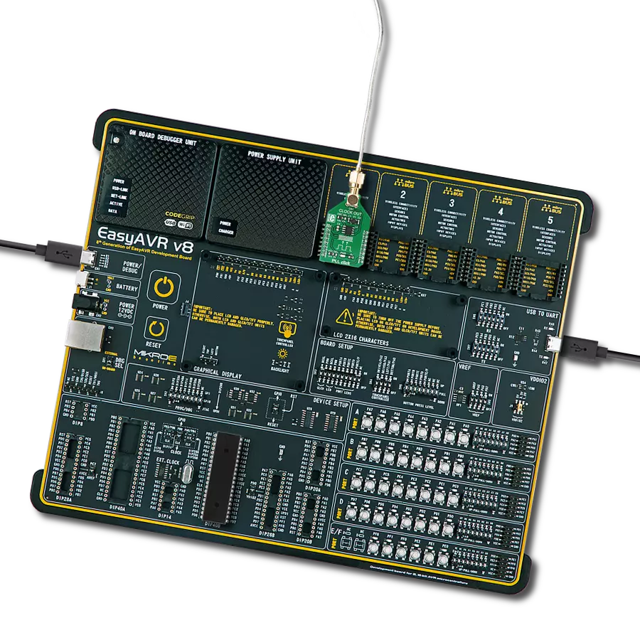
EasyAVR v8
Compiler
NECTO Studio
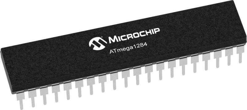
MCU
ATmega1284
Generate highly stable and coherent high-frequency signals for applications requiring tight synchronization and minimal phase noise
A
A
Hardware Overview
How does it work?
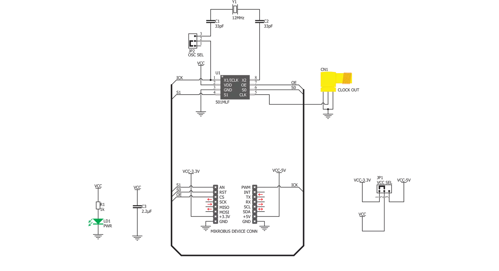
PLL Click is based on the ICS501, a LOCO™ PLL clock multiplier, from Integrated Device Technology. This IC uses the Phase-Locked Loop to provide a high-frequency clock output, deriving input from a much cheaper, standard fundamental frequency crystal oscillator. Besides the onboard crystal oscillator fixed at 12MHz, it is possible to select the signal from the mikroBUS™ PWM pin as the clock input source. To select the desired multiplication factor, the states of the two input pins, S0 and S1, are routed to the mikroBUS™ pins RST and AN, respectively. These pins can be set to a HIGH or LOW logic state or disconnected (by tri-stating the MCU pins). The combination of these pins states will set the PLL
Click to a specific multiplier. The Output Enable (OE) pin of the ICS501 is used to turn off the output clock by setting it to a LOW logic level. It will additionally set the clock output pin in high impedance (Hi-Z) mode, allowing complete disconnection and no influence on the rest of the circuit, which is useful for experimenting and prototyping purposes. This pin is internally pulled to a HIGH logic level. The OE pin is routed to the CS pin of the mikroBUS™. PLL Click is equipped with two onboard SMD jumpers. The SMD jumper labeled as the VCC SEL is used to select the operating voltage level, consequently limiting the amplitude of the clock output signal with respect to the selected voltage. The other SMD jumper
labeled as the OSC SEL chooses the clock input source between the onboard 12MHz crystal oscillator or the external clock signal. The output signal is routed through the onboard SMA connector, which provides a secure connection and good signal shielding. PLL Click has a library containing functions for all the MIKROE compilers (mikroBASIC, mikroPASCAL, and mikroC). Although relatively easy to control, the library offers comprehensive functions that make the code readable and easy to use. The included example application demonstrates the use of these functions, and it can be used as a reference for custom projects.

Features overview
Development board
EasyAVR v8 is a development board designed to rapidly develop embedded applications based on 8-bit AVR microcontrollers (MCUs). Redesigned from the ground up, EasyAVR v8 offers a familiar set of standard features, as well as some new and unique features standard for the 8th generation of development boards: programming and debugging over the WiFi network, connectivity provided by USB-C connectors, support for a wide range of different MCUs, and more. The development board is designed so that the developer has everything that might be needed for the application development, following the Swiss Army knife concept: a highly advanced programmer/debugger module, a reliable power supply module, and a USB-UART connectivity option. EasyAVR v8 board offers several different DIP sockets, covering a wide range of 8-bit AVR MCUs, from the smallest
AVR MCU devices with only eight pins, all the way up to 40-pin "giants". The development board supports the well-established mikroBUS™ connectivity standard, offering five mikroBUS™ sockets, allowing access to a huge base of Click boards™. EasyAVR v8 offers two display options, allowing even the basic 8-bit AVR MCU devices to utilize them and display graphical or textual content. One of them is the 1x20 graphical display connector, compatible with the familiar Graphical Liquid Crystal Display (GLCD) based on the KS108 (or compatible) display driver, and EasyTFT board that contains TFT Color Display MI0283QT-9A, which is driven by ILI9341 display controller, capable of showing advanced graphical content. The other option is the 2x16 character LCD module, a four-bit display module with an embedded character-based display controller. It
requires minimal processing power from the host MCU for its operation. There is a wide range of useful interactive options at the disposal: high-quality buttons with selectable press levels, LEDs, pull-up/pulldown DIP switches, and more. All these features are packed on a single development board, which uses innovative manufacturing technologies, delivering a fluid and immersive working experience. The EasyAVR v8 development board is also integral to the MIKROE rapid development ecosystem. Natively supported by the MIKROE Software toolchain, backed up by hundreds of different Click board™ designs with their number growing daily, it covers many different prototyping and development aspects, thus saving precious development time.

Microcontroller Overview
MCU Card / MCU
Architecture
AVR
MCU Memory (KB)
128
Silicon Vendor
Microchip
Pin count
40
RAM (Bytes)
16384
Used MCU Pins
mikroBUS™ mapper
Take a closer look
Click board™ Schematic
Step by step
Project assembly

Start by selecting your development board and Click board™. Begin with the EasyAVR v8 as your development board.


Track your results in real time
Application Output
1. Application Output - In Debug mode, the 'Application Output' window enables real-time data monitoring, offering direct insight into execution results. Ensure proper data display by configuring the environment correctly using the provided tutorial.

2. UART Terminal - Use the UART Terminal to monitor data transmission via a USB to UART converter, allowing direct communication between the Click board™ and your development system. Configure the baud rate and other serial settings according to your project's requirements to ensure proper functionality. For step-by-step setup instructions, refer to the provided tutorial.

3. Plot Output - The Plot feature offers a powerful way to visualize real-time sensor data, enabling trend analysis, debugging, and comparison of multiple data points. To set it up correctly, follow the provided tutorial, which includes a step-by-step example of using the Plot feature to display Click board™ readings. To use the Plot feature in your code, use the function: plot(*insert_graph_name*, variable_name);. This is a general format, and it is up to the user to replace 'insert_graph_name' with the actual graph name and 'variable_name' with the parameter to be displayed.

Software Support
Library Description
This library contains API for PLL Click driver.
Key functions:
pll_set_clock_output- This function settings clock outputpll_set_pll_4x- This function settings PLL x4pll_set_pll_6x- This function settings PLL x6
Open Source
Code example
The complete application code and a ready-to-use project are available through the NECTO Studio Package Manager for direct installation in the NECTO Studio. The application code can also be found on the MIKROE GitHub account.
/*!
 * \file
 * \brief PLL Click example
 *
 * # Description
 * This app sets PLL signals.
 *
 * The demo application is composed of two sections :
 *
 * ## Application Init
 * Initializes device.
 *
 * ## Application Task
 * Every 2 seconds, the PLL increases the input clock from min (x2) to max (x8) level.
 *
 * \author MikroE Team
 *
 */
// ------------------------------------------------------------------- INCLUDES

#include "board.h"
#include "log.h"
#include "pll.h"

// ------------------------------------------------------------------ VARIABLES

static pll_t pll;
static log_t logger;

// ------------------------------------------------------ APPLICATION FUNCTIONS

void application_init ( void )
{
    log_cfg_t log_cfg;
    pll_cfg_t cfg;

    /**
     * Logger initialization.
     * Default baud rate: 115200
     * Default log level: LOG_LEVEL_DEBUG
     * @note If USB_UART_RX and USB_UART_TX
     * are defined as HAL_PIN_NC, you will
     * need to define them manually for log to work.
     * See @b LOG_MAP_USB_UART macro definition for detailed explanation.
     */
    LOG_MAP_USB_UART( log_cfg );
    log_init( &logger, &log_cfg );
    log_info( &logger, "---- Application Init ----" );

    //  Click initialization.
    pll_cfg_setup( &cfg );
    PLL_MAP_MIKROBUS( cfg, MIKROBUS_1 );
    pll_init( &pll, &cfg );
    pll_set_clock_output( &pll, PLL_CLOCK_ENABLE );
}

void application_task ( void )
{
    log_printf( &logger, " PLL level: x2\r\n\n" );
    pll_set_pll_2x( &pll );
    Delay_ms ( 1000 );
    Delay_ms ( 1000 );
    log_printf( &logger, " PLL level: x3\r\n\n" );
    pll_set_pll_3x( &pll );
    Delay_ms ( 1000 );
    Delay_ms ( 1000 );
    log_printf( &logger, " PLL level: x3.125\r\n\n" );
    pll_set_pll_3_125x( &pll );
    Delay_ms ( 1000 );
    Delay_ms ( 1000 );
    log_printf( &logger, " PLL level: x4\r\n\n" );
    pll_set_pll_4x( &pll );
    Delay_ms ( 1000 );
    Delay_ms ( 1000 );
    log_printf( &logger, " PLL level: x5\r\n\n" );
    pll_set_pll_5x( &pll );
    Delay_ms ( 1000 );
    Delay_ms ( 1000 );
    log_printf( &logger, " PLL level: x5.3125\r\n\n" );
    pll_set_pll_5_3125x( &pll );
    Delay_ms ( 1000 );
    Delay_ms ( 1000 );
    log_printf( &logger, " PLL level: x6\r\n\n" );
    pll_set_pll_6x( &pll );
    Delay_ms ( 1000 );
    Delay_ms ( 1000 );
    log_printf( &logger, " PLL level: x6.25\r\n\n" );
    pll_set_pll_6_25x( &pll );
    Delay_ms ( 1000 );
    Delay_ms ( 1000 );
    log_printf( &logger, " PLL level: x8\r\n\n" );
    pll_set_pll_8x( &pll );
    Delay_ms ( 1000 );
    Delay_ms ( 1000 );
}

int main ( void )
{
    /* Do not remove this line or clock might not be set correctly. */
    #ifdef PREINIT_SUPPORTED
    preinit();
    #endif

    application_init( );

    for ( ; ; )
    {
        application_task( );
    }

    return 0;
}

// ------------------------------------------------------------------------ END


