Create custom A/D conversions with ADC122S101 and STM32F031K6
Make your analog signals digital

Published Oct 01, 2024
Click board™
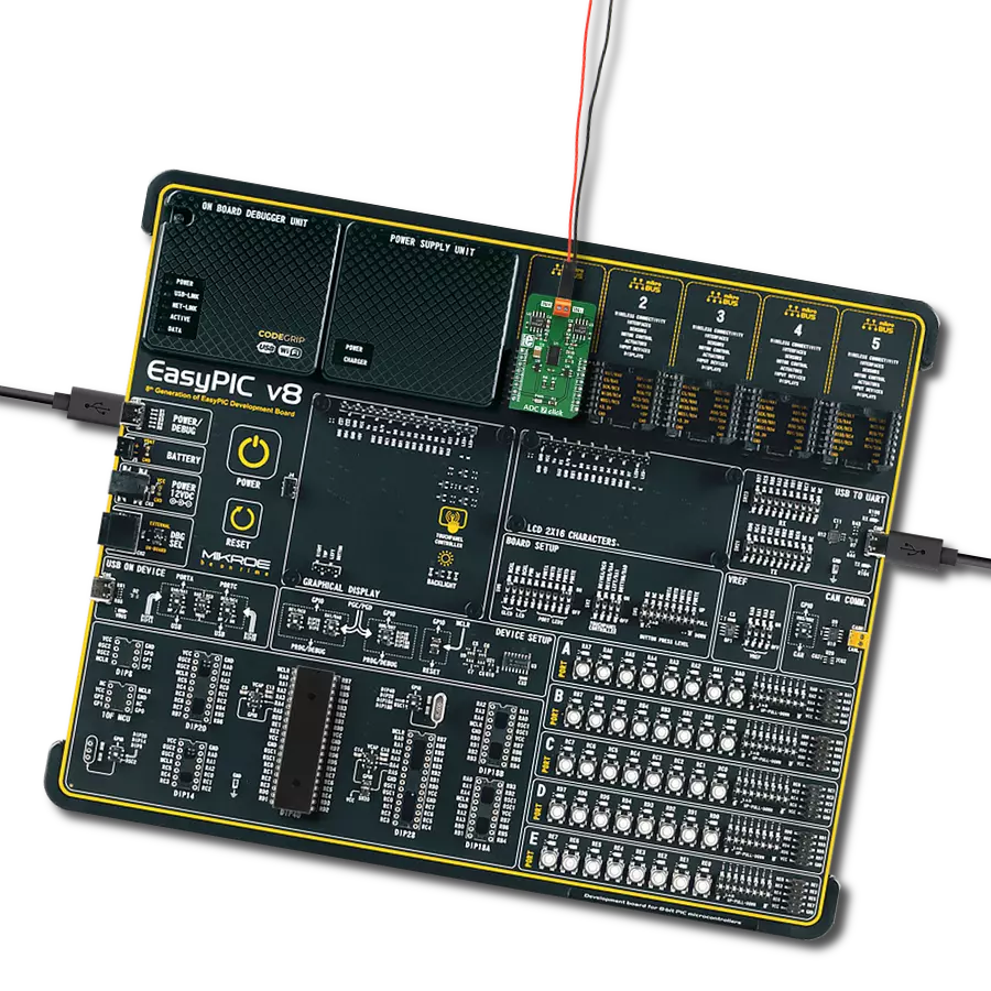
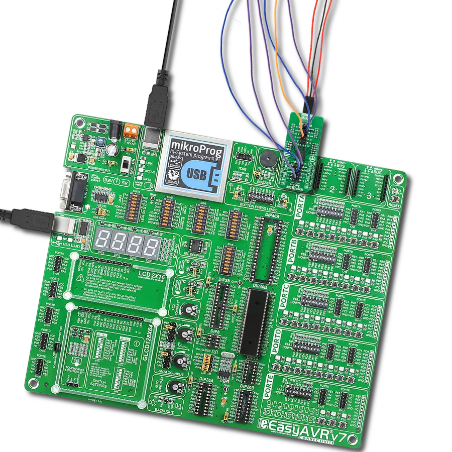
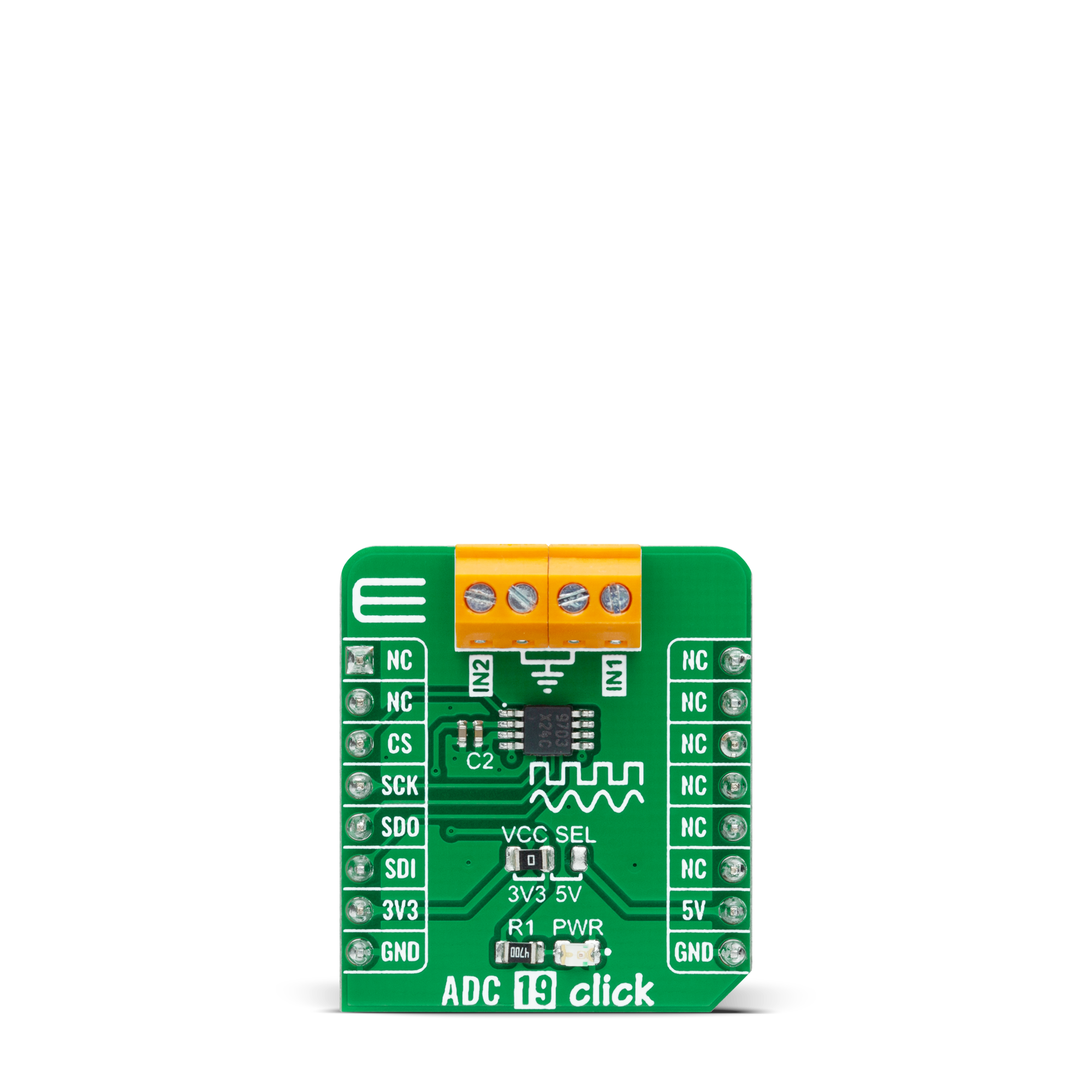
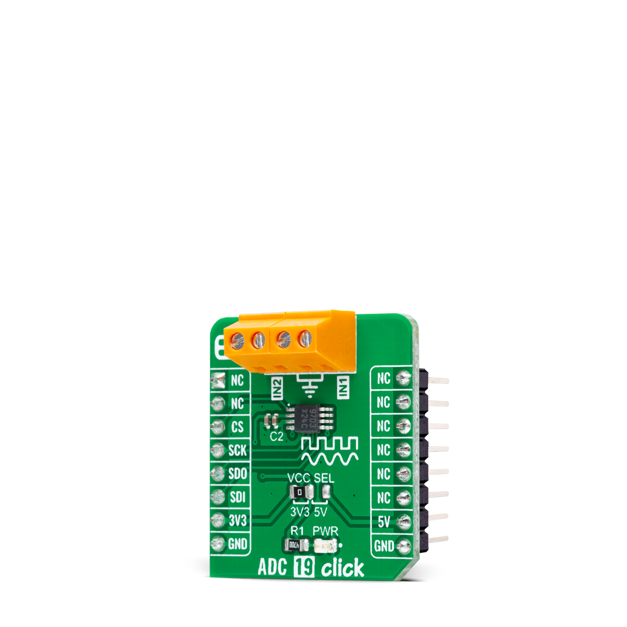
ADC 19 Click
Dev. board
Nucleo 32 with STM32F031K6 MCU
Compiler
NECTO Studio
MCU
STM32F031K6
Achieve greater efficiency and accuracy in your designs with our top-of-the-line ADC
A
A
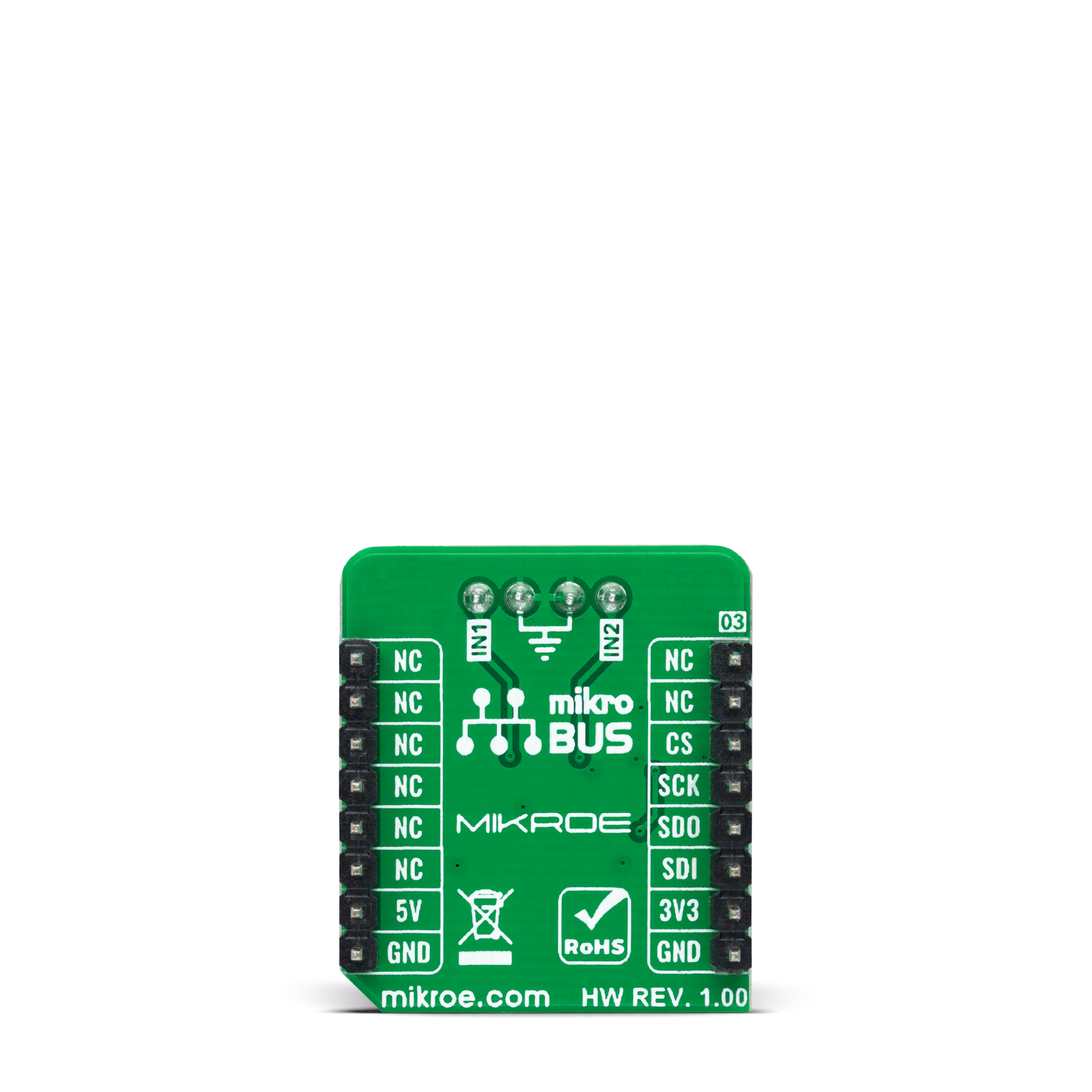
Hardware Overview
How does it work?
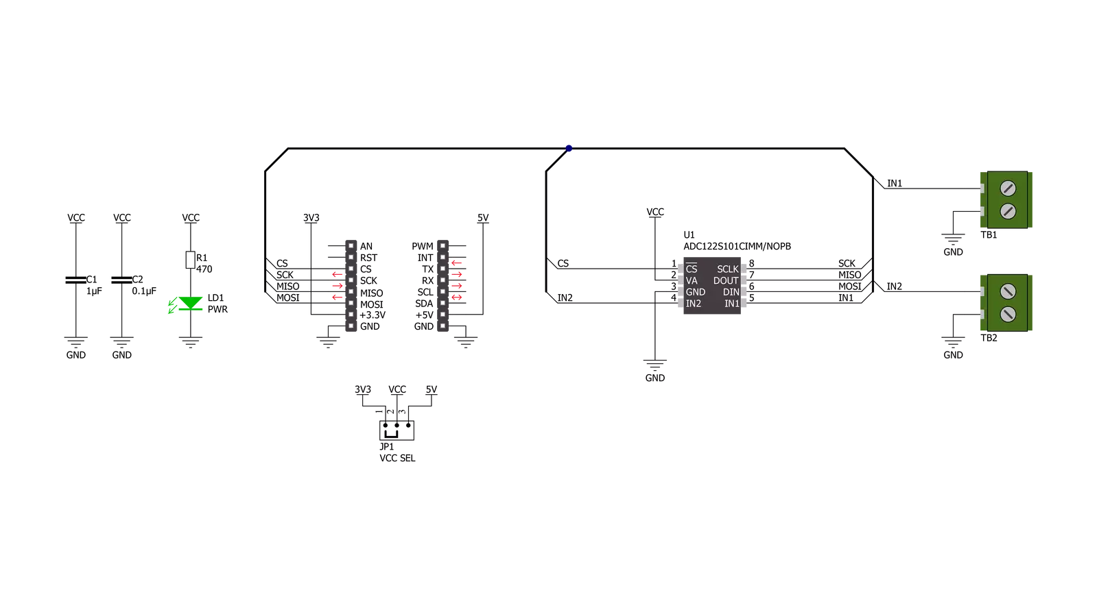
ADC 19 Click is based on the ADC122S101, a high-performance two-channel CMOS analog-to-digital converter (ADC) from Texas Instruments. The ADC122S101 has an integrated 12-bit SAR-ADC, input multiplexer, and control logic block, allowing ADC to communicate with MCU through a high-speed serial interface. Unlike the conventional practice of specifying performance at a single sample rate, this ADC is fully specified over a sample rate range of 500ksps to 1Msps.
The converter is based on a successive approximation register architecture with an internal track-and-hold circuit configurable to accept one or two input signals at its input channels. This ADC 19 Click communicates with MCU through a standard SPI interface and operates at clock rates up to 16MHz, providing data in a digital format of 12 bits. The output serial data is straight binary and is compatible with several standards, such as SPI, QSPI, MICROWIRE, and many
standard DSP serial interfaces. This Click board™ can operate with either 3.3V or 5V logic voltage levels selected via the VCC SEL jumper. This way, both 3.3V and 5V capable MCUs can use the communication lines properly. However, the Click board™ comes equipped with a library containing easy-to-use functions and an example code that can be used, as a reference, for further development.
Features overview
Development board
Nucleo 32 with STM32F031K6 MCU board provides an affordable and flexible platform for experimenting with STM32 microcontrollers in 32-pin packages. Featuring Arduino™ Nano connectivity, it allows easy expansion with specialized shields, while being mbed-enabled for seamless integration with online resources. The
board includes an on-board ST-LINK/V2-1 debugger/programmer, supporting USB reenumeration with three interfaces: Virtual Com port, mass storage, and debug port. It offers a flexible power supply through either USB VBUS or an external source. Additionally, it includes three LEDs (LD1 for USB communication, LD2 for power,
and LD3 as a user LED) and a reset push button. The STM32 Nucleo-32 board is supported by various Integrated Development Environments (IDEs) such as IAR™, Keil®, and GCC-based IDEs like AC6 SW4STM32, making it a versatile tool for developers.

Microcontroller Overview
MCU Card / MCU

Architecture
ARM Cortex-M0
MCU Memory (KB)
32
Silicon Vendor
STMicroelectronics
Pin count
32
RAM (Bytes)
4096
You complete me!
Accessories
Click Shield for Nucleo-32 is the perfect way to expand your development board's functionalities with STM32 Nucleo-32 pinout. The Click Shield for Nucleo-32 provides two mikroBUS™ sockets to add any functionality from our ever-growing range of Click boards™. We are fully stocked with everything, from sensors and WiFi transceivers to motor control and audio amplifiers. The Click Shield for Nucleo-32 is compatible with the STM32 Nucleo-32 board, providing an affordable and flexible way for users to try out new ideas and quickly create prototypes with any STM32 microcontrollers, choosing from the various combinations of performance, power consumption, and features. The STM32 Nucleo-32 boards do not require any separate probe as they integrate the ST-LINK/V2-1 debugger/programmer and come with the STM32 comprehensive software HAL library and various packaged software examples. This development platform provides users with an effortless and common way to combine the STM32 Nucleo-32 footprint compatible board with their favorite Click boards™ in their upcoming projects.

Used MCU Pins
mikroBUS™ mapper
Take a closer look
Click board™ Schematic
Step by step
Project assembly

Start by selecting your development board and Click board™. Begin with the Nucleo 32 with STM32F031K6 MCU as your development board.


Track your results in real time
Application Output
1. Application Output - In Debug mode, the 'Application Output' window enables real-time data monitoring, offering direct insight into execution results. Ensure proper data display by configuring the environment correctly using the provided tutorial.

2. UART Terminal - Use the UART Terminal to monitor data transmission via a USB to UART converter, allowing direct communication between the Click board™ and your development system. Configure the baud rate and other serial settings according to your project's requirements to ensure proper functionality. For step-by-step setup instructions, refer to the provided tutorial.

3. Plot Output - The Plot feature offers a powerful way to visualize real-time sensor data, enabling trend analysis, debugging, and comparison of multiple data points. To set it up correctly, follow the provided tutorial, which includes a step-by-step example of using the Plot feature to display Click board™ readings. To use the Plot feature in your code, use the function: plot(*insert_graph_name*, variable_name);. This is a general format, and it is up to the user to replace 'insert_graph_name' with the actual graph name and 'variable_name' with the parameter to be displayed.

Software Support
Library Description
This library contains API for ADC 19 Click driver.
Key functions:
adc19_set_vrefThis function sets the voltage reference value that will be used for voltage calculation.adc19_set_input_channelThis function sets the selected input channel active by modifying the control register.adc19_get_voltageThis function reads the voltage from the previously selected channel by using SPI serial interface.
Open Source
Code example
The complete application code and a ready-to-use project are available through the NECTO Studio Package Manager for direct installation in the NECTO Studio. The application code can also be found on the MIKROE GitHub account.
/*!
 * @file main.c
 * @brief ADC19 Click example
 *
 * # Description
 * This example demonstrates the use of ADC 19 Click board by reading
 * the voltage from the two analog input channels.
 *
 * The demo application is composed of two sections :
 *
 * ## Application Init
 * Initializes the driver and logger and sets the ADC voltage reference.
 *
 * ## Application Task
 * Reads and displays the voltage from the two analog input channels
 * on the USB UART approximately every 500ms.
 *
 * @author Stefan Filipovic
 *
 */

#include "board.h"
#include "log.h"
#include "adc19.h"

static adc19_t adc19;
static log_t logger;

void application_init ( void )
{
    log_cfg_t log_cfg;  /**< Logger config object. */
    adc19_cfg_t adc19_cfg;  /**< Click config object. */

    /**
     * Logger initialization.
     * Default baud rate: 115200
     * Default log level: LOG_LEVEL_DEBUG
     * @note If USB_UART_RX and USB_UART_TX
     * are defined as HAL_PIN_NC, you will
     * need to define them manually for log to work.
     * See @b LOG_MAP_USB_UART macro definition for detailed explanation.
     */
    LOG_MAP_USB_UART( log_cfg );
    log_init( &logger, &log_cfg );
    log_info( &logger, " Application Init " );

    // Click initialization.
    adc19_cfg_setup( &adc19_cfg );
    ADC19_MAP_MIKROBUS( adc19_cfg, MIKROBUS_1 );
    if ( SPI_MASTER_ERROR == adc19_init( &adc19, &adc19_cfg ) )
    {
        log_error( &logger, " Communication init." );
        for ( ; ; );
    }

    adc19_set_vref ( &adc19, ADC19_VREF_3V3 );

    log_info( &logger, " Application Task " );
}

void application_task ( void )
{
    float voltage;
    if ( ADC19_OK == adc19_set_input_channel ( &adc19, ADC19_INPUT_CHANNEL_1 ) )
    {
        if ( ADC19_OK == adc19_get_voltage ( &adc19, &voltage ) )
        {
            log_printf ( &logger, " IN1 : %.3f V \r\n", voltage );
        }
    }
    if ( ADC19_OK == adc19_set_input_channel ( &adc19, ADC19_INPUT_CHANNEL_2 ) )
    {
        if ( ADC19_OK == adc19_get_voltage ( &adc19, &voltage ) )
        {
            log_printf ( &logger, " IN2 : %.3f V \r\n\n", voltage );
        }
    }
    Delay_ms ( 500 );
}

int main ( void )
{
    /* Do not remove this line or clock might not be set correctly. */
    #ifdef PREINIT_SUPPORTED
    preinit();
    #endif

    application_init( );

    for ( ; ; )
    {
        application_task( );
    }

    return 0;
}

// ------------------------------------------------------------------------ END