Keep your data protected and secure with AT25FF321A and TM4C1294NCZAD
A flash that never fades!

Published Mar 11, 2023
Click board™
Flash 10 Click
Dev. board
Fusion for Tiva v8
Compiler
NECTO Studio
MCU
TM4C1294NCZAD
Keep data and information stored even when the power is off
A
A
Hardware Overview
How does it work?
Flash 10 Click is based on the AT25FF321A, a highly reliable serial Flash memory solution designed for use in various high-volume consumer and connected applications from Dialog Semiconductor. The AT25FF321A is organized as a 32Mbit (16x2 Mbit physical block) Flash memory ideally suited for systems where program code is shadowed from Flash memory into embedded or external RAM (code shadow) for execution and where small amounts of data are stored and updated locally in the Flash memory. The AT25FF321A specifies a minimum of 100.000 endurance cycles with data retention of a minimum of 20 years, allowing it to handle unlimited reads/writes to the memory. The AT25FF321A's erase block sizes are optimized to meet the needs of today's code and data storage applications, supporting flexible and optimized erase architecture for code and data storage
applications (4kB, 32kB, and 64kB block erase operations) and a full-chip erase feature. Optimizing the erase blocks' size can be the most efficient use of memory space. Also, the AT25FF321A contains four specialized 128-byte One-Time Programmable (OTP) security registers which can be used to store a unique device ID and locked key storage. Flash 10 Click communicates with MCU through a standard SPI interface supporting the two most common SPI modes, SPI Mode 0 and 3. Furthermore, this Click board™ provides additional hardware-controlled functions. The configurable Write Protection, marked as WP and routed on the PWM pin of the mikroBUS™ socket, protects all registers (including status and configuration) from write operations and must be held low to inhibit all the write operations to registers. When this pin is low, all memory and register write
operations are prohibited, and the address counter is not incremented. Also, it is possible to use the Reset or Hold function through the RST pin of the mikroBUS™ socket, depending on the state of the HOLD/RESET bit 7 in Status Register 3. In the case of the Hold function, this pin temporarily pauses serial communication without deselecting or resetting the device, while in the case of the Reset feature, a low logic level on the RST pin puts the AT25FF321A into a Reset state. This Click board™ can only be operated with a 3.3V logic voltage level. The board must perform appropriate logic voltage level conversion before using MCUs with different logic levels. However, the Click board™ comes equipped with a library containing functions and an example code that can be used as a reference for further development.


Features overview
Development board
Fusion for TIVA v8 is a development board specially designed for the needs of rapid development of embedded applications. It supports a wide range of microcontrollers, such as different 32-bit ARM® Cortex®-M based MCUs from Texas Instruments, regardless of their number of pins, and a broad set of unique functions, such as the first-ever embedded debugger/programmer over a WiFi network. The development board is well organized and designed so that the end-user has all the necessary elements, such as switches, buttons, indicators, connectors, and others, in one place. Thanks to innovative manufacturing technology, Fusion for TIVA v8 provides a fluid and immersive working experience, allowing access
anywhere and under any circumstances at any time. Each part of the Fusion for TIVA v8 development board contains the components necessary for the most efficient operation of the same board. An advanced integrated CODEGRIP programmer/debugger module offers many valuable programming/debugging options, including support for JTAG, SWD, and SWO Trace (Single Wire Output)), and seamless integration with the Mikroe software environment. Besides, it also includes a clean and regulated power supply module for the development board. It can use a wide range of external power sources, including a battery, an external 12V power supply, and a power source via the USB Type-C (USB-C) connector.
Communication options such as USB-UART, USB HOST/DEVICE, CAN (on the MCU card, if supported), and Ethernet is also included. In addition, it also has the well-established mikroBUS™ standard, a standardized socket for the MCU card (SiBRAIN standard), and two display options for the TFT board line of products and character-based LCD. Fusion for TIVA v8 is an integral part of the Mikroe ecosystem for rapid development. Natively supported by Mikroe software tools, it covers many aspects of prototyping and development thanks to a considerable number of different Click boards™ (over a thousand boards), the number of which is growing every day.

Microcontroller Overview
MCU Card / MCU
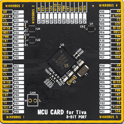
Type
8th Generation
Architecture
ARM Cortex-M4
MCU Memory (KB)
1024
Silicon Vendor
Texas Instruments
Pin count
212
RAM (Bytes)
262144
Used MCU Pins
mikroBUS™ mapper
Take a closer look
Click board™ Schematic

Step by step
Project assembly

Start by selecting your development board and Click board™. Begin with the Fusion for Tiva v8 as your development board.


Track your results in real time
Application Output
1. Application Output - In Debug mode, the 'Application Output' window enables real-time data monitoring, offering direct insight into execution results. Ensure proper data display by configuring the environment correctly using the provided tutorial.

2. UART Terminal - Use the UART Terminal to monitor data transmission via a USB to UART converter, allowing direct communication between the Click board™ and your development system. Configure the baud rate and other serial settings according to your project's requirements to ensure proper functionality. For step-by-step setup instructions, refer to the provided tutorial.

3. Plot Output - The Plot feature offers a powerful way to visualize real-time sensor data, enabling trend analysis, debugging, and comparison of multiple data points. To set it up correctly, follow the provided tutorial, which includes a step-by-step example of using the Plot feature to display Click board™ readings. To use the Plot feature in your code, use the function: plot(*insert_graph_name*, variable_name);. This is a general format, and it is up to the user to replace 'insert_graph_name' with the actual graph name and 'variable_name' with the parameter to be displayed.

Software Support
Library Description
This library contains API for Flash 10 Click driver.
Key functions:
flash10_erase_memoryThis function erases the selected amount of memory which contains the selected address.flash10_memory_writeThis function writes a desired number of data bytes starting from the selected memory address.flash10_memory_readThis function reads a desired number of data bytes starting from the selected memory address.
Open Source
Code example
The complete application code and a ready-to-use project are available through the NECTO Studio Package Manager for direct installation in the NECTO Studio. The application code can also be found on the MIKROE GitHub account.
/*!
 * @file main.c
 * @brief Flash 10 Click example
 *
 * # Description
 * This example demonstrates the use of Flash 10 Click board by writing specified data to
 * the memory and reading it back.
 *
 * The demo application is composed of two sections :
 *
 * ## Application Init
 * Initializes the driver and checks the communication by reading and verifying the device ID.
 *
 * ## Application Task
 * Writes a desired number of bytes to the memory and then verifies if it is written correctly
 * by reading from the same memory location and displaying the memory content on the USB UART.
 * The whole 4KB block of memory that contains the STARTING_ADDRESS will be erased before writing data.
 *
 * @author Stefan Filipovic
 *
 */

#include "board.h"
#include "log.h"
#include "flash10.h"

#define DEMO_TEXT_MESSAGE_1         "MIKROE"
#define DEMO_TEXT_MESSAGE_2         "Flash 10 Click"
#define STARTING_ADDRESS            0x012345

static flash10_t flash10;
static log_t logger;

void application_init ( void )
{
    log_cfg_t log_cfg;  /**< Logger config object. */
    flash10_cfg_t flash10_cfg;  /**< Click config object. */

    /**
     * Logger initialization.
     * Default baud rate: 115200
     * Default log level: LOG_LEVEL_DEBUG
     * @note If USB_UART_RX and USB_UART_TX
     * are defined as HAL_PIN_NC, you will
     * need to define them manually for log to work.
     * See @b LOG_MAP_USB_UART macro definition for detailed explanation.
     */
    LOG_MAP_USB_UART( log_cfg );
    log_init( &logger, &log_cfg );
    log_info( &logger, " Application Init " );

    // Click initialization.
    flash10_cfg_setup( &flash10_cfg );
    FLASH10_MAP_MIKROBUS( flash10_cfg, MIKROBUS_1 );
    if ( SPI_MASTER_ERROR == flash10_init( &flash10, &flash10_cfg ) )
    {
        log_error( &logger, " Communication init." );
        for ( ; ; );
    }

    if ( FLASH10_ERROR == flash10_check_communication ( &flash10 ) )
    {
        log_error( &logger, " Check communication." );
        for ( ; ; );
    }

    log_info( &logger, " Application Task " );
}

void application_task ( void )
{
    uint8_t data_buf[ 128 ] = { 0 };
    log_printf ( &logger, " Memory address: 0x%.6LX\r\n", ( uint32_t ) STARTING_ADDRESS );
    if ( FLASH10_OK == flash10_erase_memory ( &flash10, FLASH10_CMD_BLOCK_ERASE_4KB, STARTING_ADDRESS ) )
    {
        log_printf ( &logger, " Erase memory block (4KB)\r\n" );
    }
    memcpy ( data_buf, DEMO_TEXT_MESSAGE_1, strlen ( DEMO_TEXT_MESSAGE_1 ) );
    if ( FLASH10_OK == flash10_memory_write ( &flash10, STARTING_ADDRESS,
                                              data_buf, sizeof ( data_buf ) ) )
    {
        log_printf ( &logger, " Write data: %s\r\n", data_buf );
        Delay_ms ( 100 );
    }
    memset ( data_buf, 0, sizeof ( data_buf ) );
    if ( FLASH10_OK == flash10_memory_read ( &flash10, STARTING_ADDRESS,
                                             data_buf, sizeof ( data_buf ) ) )
    {
        log_printf ( &logger, " Read data: %s\r\n\n", data_buf );
        Delay_ms ( 1000 );
        Delay_ms ( 1000 );
        Delay_ms ( 1000 );
    }
    log_printf ( &logger, " Memory address: 0x%.6LX\r\n", ( uint32_t ) STARTING_ADDRESS );
    if ( FLASH10_OK == flash10_erase_memory ( &flash10, FLASH10_CMD_BLOCK_ERASE_4KB, STARTING_ADDRESS ) )
    {
        log_printf ( &logger, " Erase memory block (4KB)\r\n" );
    }
    memcpy ( data_buf, DEMO_TEXT_MESSAGE_2, strlen ( DEMO_TEXT_MESSAGE_2 ) );
    if ( FLASH10_OK == flash10_memory_write ( &flash10, STARTING_ADDRESS,
                                              data_buf, sizeof ( data_buf ) ) )
    {
        log_printf ( &logger, " Write data: %s\r\n", data_buf );
        Delay_ms ( 100 );
    }
    memset ( data_buf, 0, sizeof ( data_buf ) );
    if ( FLASH10_OK == flash10_memory_read ( &flash10, STARTING_ADDRESS,
                                             data_buf, sizeof ( data_buf ) ) )
    {
        log_printf ( &logger, " Read data: %s\r\n\n", data_buf );
        Delay_ms ( 1000 );
        Delay_ms ( 1000 );
        Delay_ms ( 1000 );
    }
}

int main ( void )
{
    /* Do not remove this line or clock might not be set correctly. */
    #ifdef PREINIT_SUPPORTED
    preinit();
    #endif

    application_init( );

    for ( ; ; )
    {
        application_task( );
    }

    return 0;
}

// ------------------------------------------------------------------------ END


