Save important data easily with S25FL512S and STM32F031K6
Faster, smarter, flashier!

Published Oct 01, 2024
Click board™
Flash 4 Click
Dev. board
Nucleo 32 with STM32F031K6 MCU
Compiler
NECTO Studio
MCU
STM32F031K6
Utilize flash memory's rapid read and write speeds for quicker data retrieval and seamless multitasking
A
A
Hardware Overview
How does it work?
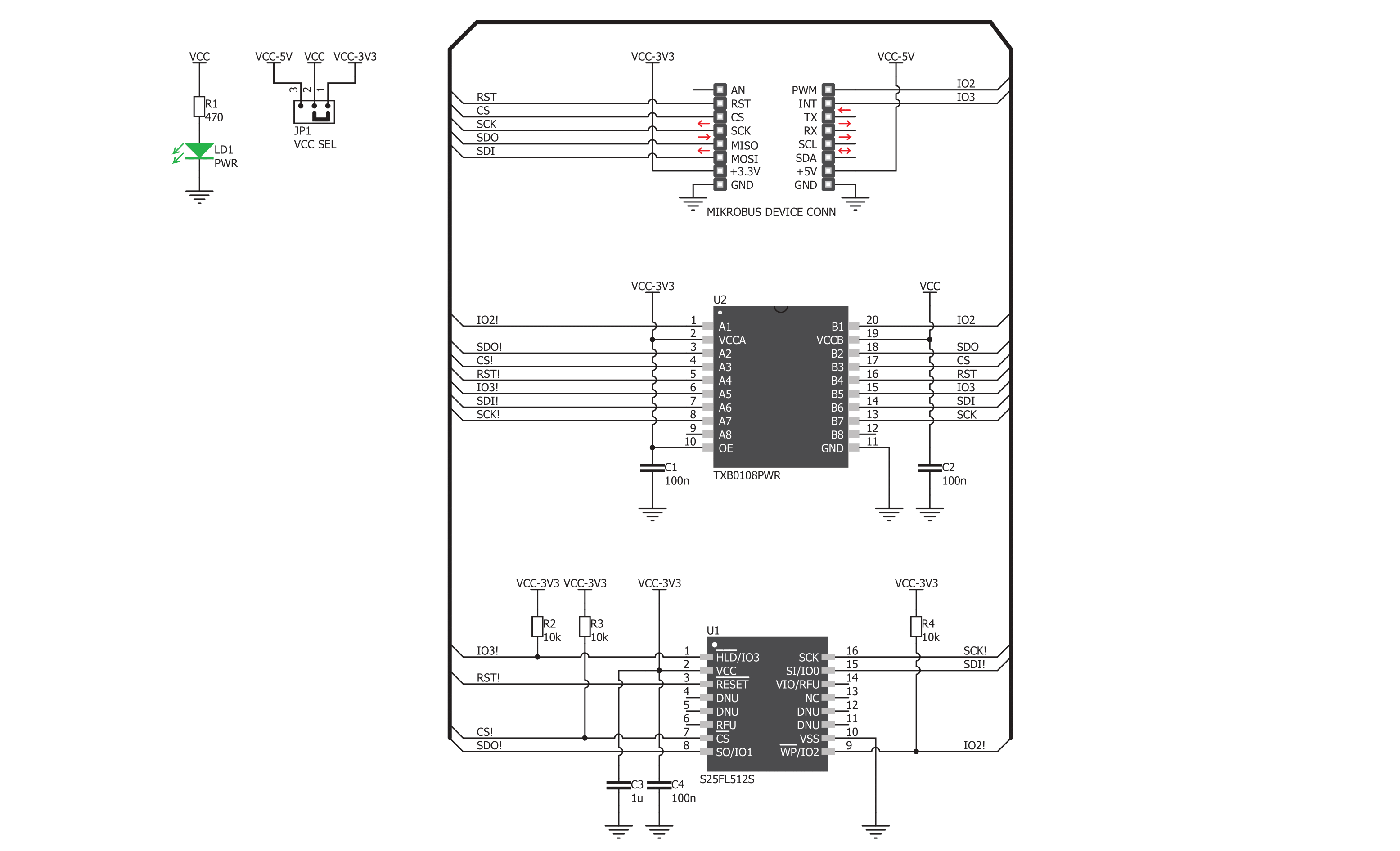
Flash 4 Click is based on Infineon's S25FL512S, a 512 Mbit SPI Flash memory module. The Flash memory density is usually expressed in bits, so 512 Mbit of memory aligned in 8 bits long words translates to a capacity of 64 megabytes (MB). This memory module contains 256 sectors of 256 KB each. Furthermore, the memory is organized in 256KB sectors, allowing users to erase the whole sector only and write up to 512 bytes at a time. The advanced MirrorBit® technology allows storing two data bits in each memory array transistor (memory cell), effectively doubling the capacity of a single storage cell. The Eclipse™ architecture is responsible for the greatly improved erase and programming performance compared to other Flash modules of the previous generation. Due to a higher speed, an execute-in-place (XIP) and data shadowing are possible with the Flash 4 Click. The S25FL512S flash module supports the standard SPI interface, but it can also optionally use the Dual and Quad SPI interface, allowing the full data transfer rate of 80MB/sec. In addition, the flash module supports DDR read commands in all SPI modes, using both clock edges to transfer the data (data transfer is performed on both the rising and the falling edge of the clock). A typical communication procedure consists of sending a proper instruction (command) from the host MCU via the SPI interface, followed by either an address,
data, or both, and a response from the S25FL512S flash module, which can be either a stream of data or a single byte, depending on the command received. One of the key features of the S25FL512S is certainly the AutoBoot feature. It allows the module to automatically initiate the memory transfer from the predefined location (memory read operation) after the reset cycle. Considering a typical communication scenario, where the READ command followed by one or more address bytes need to be used, AutoBoot allows the host MCU to pull down the #CS (Chip Select) pin and start receiving a data stream over the SPI interface for as long as the #CS pin is held LOW, without any wasted cycles. As soon as the #CS pin is released, the S25FL512S returns to normal operation. The #WP write protect pin puts the device into the hardware write protect mode. A LOW logic level on this pin prohibits writing operations to the Block-Protection bits of the Status register. Locking down the Status Register will block changes of the Status Register Write Disable (SRWD) bit, which is required for the Write and Erase operations, effectively preventing the memory content changes. The pin is multiplexed with the IO2 function. Therefore, it is not available when Quad SPI is used. The #HOLD pin is used to hold the data transfer. When the Chip Select pin (#CS, routed to the mikroBUS™ CS pin) is set
to a LOW logic level, the data transfer will be put on hold when the LOW logic level of the serial clock coincides with the falling edge of the #HOLD pin. Similarly, resuming the data transfer will happen when the LOW logic level of the serial clock coincides with the rising edge of the #HOLD pin. The pin is multiplexed with the IO3 function. Therefore it is not available when Quad SPI is used. The SPI interface pins are routed to the mikroBUS™ so that the interfacing with the microcontroller unit (MCU) is easy and straightforward. Additional pins routed to the mikroBUS™ include the #WP/IO2 pin routed to the mikroBUS™ PWM pin and labeled as IO2 and the #HOLD/IO3 pin routed to the mikroBUS™ INT pin and labeled as IO3. There is also the RESET pin, routed to the RST pin of the mikroBUS™, which performs a reset of the Flash module, initiating an AutoBoot sequence if enabled. This Click board™ can operate with either 3.3V or 5V logic voltage levels selected via the VCC SEL jumper. This way, both 3.3V and 5V capable MCUs can use the communication lines properly. Also, this Click board™ comes equipped with a library containing easy-to-use functions and an example code that can be used, as a reference, for further development.


Features overview
Development board
Nucleo 32 with STM32F031K6 MCU board provides an affordable and flexible platform for experimenting with STM32 microcontrollers in 32-pin packages. Featuring Arduino™ Nano connectivity, it allows easy expansion with specialized shields, while being mbed-enabled for seamless integration with online resources. The
board includes an on-board ST-LINK/V2-1 debugger/programmer, supporting USB reenumeration with three interfaces: Virtual Com port, mass storage, and debug port. It offers a flexible power supply through either USB VBUS or an external source. Additionally, it includes three LEDs (LD1 for USB communication, LD2 for power,
and LD3 as a user LED) and a reset push button. The STM32 Nucleo-32 board is supported by various Integrated Development Environments (IDEs) such as IAR™, Keil®, and GCC-based IDEs like AC6 SW4STM32, making it a versatile tool for developers.

Microcontroller Overview
MCU Card / MCU

Architecture
ARM Cortex-M0
MCU Memory (KB)
32
Silicon Vendor
STMicroelectronics
Pin count
32
RAM (Bytes)
4096
You complete me!
Accessories
Click Shield for Nucleo-32 is the perfect way to expand your development board's functionalities with STM32 Nucleo-32 pinout. The Click Shield for Nucleo-32 provides two mikroBUS™ sockets to add any functionality from our ever-growing range of Click boards™. We are fully stocked with everything, from sensors and WiFi transceivers to motor control and audio amplifiers. The Click Shield for Nucleo-32 is compatible with the STM32 Nucleo-32 board, providing an affordable and flexible way for users to try out new ideas and quickly create prototypes with any STM32 microcontrollers, choosing from the various combinations of performance, power consumption, and features. The STM32 Nucleo-32 boards do not require any separate probe as they integrate the ST-LINK/V2-1 debugger/programmer and come with the STM32 comprehensive software HAL library and various packaged software examples. This development platform provides users with an effortless and common way to combine the STM32 Nucleo-32 footprint compatible board with their favorite Click boards™ in their upcoming projects.

Used MCU Pins
mikroBUS™ mapper
Take a closer look
Click board™ Schematic
Step by step
Project assembly

Start by selecting your development board and Click board™. Begin with the Nucleo 32 with STM32F031K6 MCU as your development board.


Software Support
Library Description
This library contains API for Flash 4 Click driver.
Key functions:
flash4_read_manufacturer_id- Function for read Manufacturer IDflash4_write_command- Write command functionflash4_read_flash_4- Read Flash with 4 byte address function
Open Source
Code example
The complete application code and a ready-to-use project are available through the NECTO Studio Package Manager for direct installation in the NECTO Studio. The application code can also be found on the MIKROE GitHub account.
/*!
 * \file
 * \brief Flash4 Click example
 *
 * # Description
 * This example demonstrates the use of Flash 4 Click board.
 *
 * The demo application is composed of two sections :
 *
 * ## Application Init
 * Initializes the driver and enables the Click board, then checks the communication
 * by reading the device and manufacturer IDs.
 *
 * ## Application Task
 * Erases sector memory starting from 0x00001234 address, then writes a desired message
 * to the same address. After that, verifies if the message is written correctly by reading
 * it back and displaying it to the USB UART every 5 seconds.
 *
 * \author MikroE Team
 *
 */
// ------------------------------------------------------------------- INCLUDES

#include "board.h"
#include "log.h"
#include "flash4.h"

// ------------------------------------------------------------------ VARIABLES

#define DEMO_MESSAGE "MikroE"

static flash4_t flash4;
static log_t logger;

static uint8_t device_id[ 2 ];
// ------------------------------------------------------ APPLICATION FUNCTIONS

void application_init ( void )
{
    log_cfg_t log_cfg;
    flash4_cfg_t cfg;

    /**
     * Logger initialization.
     * Default baud rate: 115200
     * Default log level: LOG_LEVEL_DEBUG
     * @note If USB_UART_RX and USB_UART_TX
     * are defined as HAL_PIN_NC, you will
     * need to define them manually for log to work.
     * See @b LOG_MAP_USB_UART macro definition for detailed explanation.
     */
    LOG_MAP_USB_UART( log_cfg );
    log_init( &logger, &log_cfg );
    log_info( &logger, "---- Application Init ----" );

    //  Click initialization.

    flash4_cfg_setup( &cfg );
    FLASH4_MAP_MIKROBUS( cfg, MIKROBUS_1 );
    flash4_init( &flash4, &cfg );

    flash4_reset( &flash4 );

    Delay_ms ( 1000 );

    flash4_read_manufacturer_id( &flash4, device_id );

    if ( device_id[ 0 ] != FLASH4_MANUFACTURER_ID || device_id[ 1 ] != FLASH4_DEVICE_ID )
    {
        log_error( &logger, "WRONG ID READ" );
        log_printf( &logger, "Please restart your system.\r\n" );
        for( ; ; );
    }
    Delay_ms ( 1000 );
}

void application_task ( void )
{
    char read_buffer[ 10 ] = { 0 };

    flash4_write_command( &flash4, FLASH4_CMD_WRITE_ENABLE_WREN );
    log_printf( &logger, "--- Erase chip --START-- \r\n" );
    flash4_sector_erase_4( &flash4,  0x00001234 );
    while ( flash4_check_wip( &flash4 ) );
    log_printf( &logger, "--- Erase chip --DONE-- \r\n" );

    flash4_write_command( &flash4, FLASH4_CMD_WRITE_ENABLE_WREN );
    flash4_page_program_4( &flash4, DEMO_MESSAGE, 0x00001234, strlen( DEMO_MESSAGE ) );
    while ( flash4_check_wip( &flash4 ) );
    Delay_100ms( );

    flash4_read_flash_4( &flash4, read_buffer, 0x00001234, strlen( DEMO_MESSAGE ) );
    while ( flash4_check_wip( &flash4 ) );

    log_printf( &logger, "--- Read buffer : %s\r\n", read_buffer );

    Delay_ms ( 1000 );
    Delay_ms ( 1000 );
    Delay_ms ( 1000 );
    Delay_ms ( 1000 );
    Delay_ms ( 1000 );
}

int main ( void )
{
    /* Do not remove this line or clock might not be set correctly. */
    #ifdef PREINIT_SUPPORTED
    preinit();
    #endif

    application_init( );

    for ( ; ; )
    {
        application_task( );
    }

    return 0;
}


// ------------------------------------------------------------------------ END
Additional Support
Resources
Category:FLASH


