Enhance system performance with high-speed flash storage using IS25LP128 and PIC18F57Q43
Embrace the future with flash storage

Published Feb 13, 2024
Click board™
Flash 3 Click
Dev. board
Curiosity Nano with PIC18F57Q43
Compiler
NECTO Studio
MCU
PIC18F57Q43
Employ flash memory to boost overall system responsiveness and application loading times
A
A
Hardware Overview
How does it work?
Flash 3 Click is based on the IS25LP128, a serial Flash memory with 133MHz multi I/O SPI & quad I/O QPI DTR interfaces from Integrated Silicon Solution. This Flash memory chip supports Serial Flash Discoverable Parameters (SFDP), selectable dummy cycles, SPI modes 0 and 3, and configurable drive strength. The flexible and efficient memory architecture allows chip erase with uniform sector/block erase (4/32/64 KB) and program/erase suspend and resume. The read and program modes consist of low instruction overhead operations, continuous read 8/16/32/64-byte burst wrap, selectable burst length,
and more. There are software and hardware protections, power supply lock protection, a 4x256-byte dedicated security area with OTP user-lockable bits, and the 128-bit Unique ID for each device. The Flash 3 Click communicates with the host MCU through an industry-standard SPI serial interface, supporting the two most common SPI modes, SPI Mode 0 and 3, with a maximum frequency of 133MHz in Fast Read mode. The Flash 3 Click features write-protect ability over the WP pin, with active LOW. The HLD pin is a communication hold pin, and the Flash memory can stay in a hold state with logic LOW, in which
time the device is paused without resetting the serial sequence. The CE pin turns the device’s operation on and off on this Click board™, pulled high for normal operation. This Click board™ can be operated only with a 3.3V logic voltage level. The board must perform appropriate logic voltage level conversion before using MCUs with different logic levels. Also, it comes equipped with a library containing functions and an example code that can be used, as a reference, for further development.


Features overview
Development board
PIC18F57Q43 Curiosity Nano evaluation kit is a cutting-edge hardware platform designed to evaluate microcontrollers within the PIC18-Q43 family. Central to its design is the inclusion of the powerful PIC18F57Q43 microcontroller (MCU), offering advanced functionalities and robust performance. Key features of this evaluation kit include a yellow user LED and a responsive
mechanical user switch, providing seamless interaction and testing. The provision for a 32.768kHz crystal footprint ensures precision timing capabilities. With an onboard debugger boasting a green power and status LED, programming and debugging become intuitive and efficient. Further enhancing its utility is the Virtual serial port (CDC) and a debug GPIO channel (DGI
GPIO), offering extensive connectivity options. Powered via USB, this kit boasts an adjustable target voltage feature facilitated by the MIC5353 LDO regulator, ensuring stable operation with an output voltage ranging from 1.8V to 5.1V, with a maximum output current of 500mA, subject to ambient temperature and voltage constraints.

Microcontroller Overview
MCU Card / MCU

Architecture
PIC
MCU Memory (KB)
128
Silicon Vendor
Microchip
Pin count
48
RAM (Bytes)
8196
You complete me!
Accessories
Curiosity Nano Base for Click boards is a versatile hardware extension platform created to streamline the integration between Curiosity Nano kits and extension boards, tailored explicitly for the mikroBUS™-standardized Click boards and Xplained Pro extension boards. This innovative base board (shield) offers seamless connectivity and expansion possibilities, simplifying experimentation and development. Key features include USB power compatibility from the Curiosity Nano kit, alongside an alternative external power input option for enhanced flexibility. The onboard Li-Ion/LiPo charger and management circuit ensure smooth operation for battery-powered applications, simplifying usage and management. Moreover, the base incorporates a fixed 3.3V PSU dedicated to target and mikroBUS™ power rails, alongside a fixed 5.0V boost converter catering to 5V power rails of mikroBUS™ sockets, providing stable power delivery for various connected devices.

Used MCU Pins
mikroBUS™ mapper
Take a closer look
Click board™ Schematic

Step by step
Project assembly

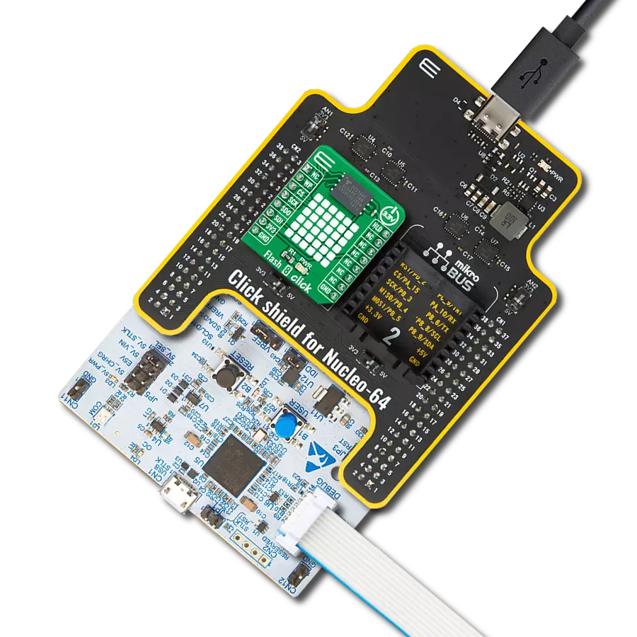
Start by selecting your development board and Click board™. Begin with the Curiosity Nano with PIC18F57Q43 as your development board.


Track your results in real time
Application Output
1. Application Output - In Debug mode, the 'Application Output' window enables real-time data monitoring, offering direct insight into execution results. Ensure proper data display by configuring the environment correctly using the provided tutorial.

2. UART Terminal - Use the UART Terminal to monitor data transmission via a USB to UART converter, allowing direct communication between the Click board™ and your development system. Configure the baud rate and other serial settings according to your project's requirements to ensure proper functionality. For step-by-step setup instructions, refer to the provided tutorial.

3. Plot Output - The Plot feature offers a powerful way to visualize real-time sensor data, enabling trend analysis, debugging, and comparison of multiple data points. To set it up correctly, follow the provided tutorial, which includes a step-by-step example of using the Plot feature to display Click board™ readings. To use the Plot feature in your code, use the function: plot(*insert_graph_name*, variable_name);. This is a general format, and it is up to the user to replace 'insert_graph_name' with the actual graph name and 'variable_name' with the parameter to be displayed.

Software Support
Library Description
This library contains API for Flash 3 Click driver.
Key functions:
flash3_pause- Pause functionflash3_unpause- Unpause function
Open Source
Code example
The complete application code and a ready-to-use project are available through the NECTO Studio Package Manager for direct installation in the NECTO Studio. The application code can also be found on the MIKROE GitHub account.
/*!
 * \file
 * \brief Flash3 Click example
 *
 * # Description
 * This applicaion adding more flash memory.
 *
 * The demo application is composed of two sections :
 *
 * ## Application Init
 * Initalizes device, Flash 3 Click board and makes an initial log.
 *
 * ## Application Task
 * This is an example that shows the capabilities of the Flash 3 Click by
   writing into memory array of a Flash 3 Click board and reading same data from memory array.
 *
 * \author MikroE Team
 *
 */
// ------------------------------------------------------------------- INCLUDES

#include "board.h"
#include "log.h"
#include "flash3.h"

// ------------------------------------------------------------------ VARIABLES

static flash3_t flash3;
static log_t logger;

// ------------------------------------------------------ APPLICATION FUNCTIONS

void application_init ( void )
{
    log_cfg_t log_cfg;
    flash3_cfg_t cfg;

    /**
     * Logger initialization.
     * Default baud rate: 115200
     * Default log level: LOG_LEVEL_DEBUG
     * @note If USB_UART_RX and USB_UART_TX
     * are defined as HAL_PIN_NC, you will
     * need to define them manually for log to work.
     * See @b LOG_MAP_USB_UART macro definition for detailed explanation.
     */
    LOG_MAP_USB_UART( log_cfg );
    log_init( &logger, &log_cfg );
    log_info( &logger, "---- Application Init ----" );

    //  Click initialization.

    flash3_cfg_setup( &cfg );
    FLASH3_MAP_MIKROBUS( cfg, MIKROBUS_1 );
    flash3_init( &flash3, &cfg );

    Delay_ms ( 100 );
    log_printf( &logger, "------------------- \r\n" );
    log_printf( &logger, "  Flash  3  Click  \r\n" );
    log_printf( &logger, "-------------------\r\n" );
    flash3_setting( &flash3 );
    Delay_ms ( 100 );
    log_printf( &logger, "   Initialized     \r\n" );
    log_printf( &logger, "------------------- \r\n" );
}

void application_task ( void )
{
    char val_in[ 8 ] = { 0x4D, 0x49, 0x4B, 0x52, 0x4F, 0x45, 0x00 };
    char val_out[ 8 ] = { 0 };

    log_printf( &logger, "\r\n ____________________ \r\n" );
    log_printf( &logger, "Begin demonstration! \r\n\r\n" );


    log_printf( &logger, "Writing : %s\r\n", val_in );
    flash3_write( &flash3, 0x000000, &val_in[ 0 ], 6 );
    Delay_ms ( 100 );
    log_printf( &logger, "------------------ \r\n" );

    log_printf( &logger, "Reading : %s\r\n", val_in );
    flash3_normal_read( &flash3, 0x000000, &val_in[ 0 ], 6 );
    Delay_ms ( 100 );
    log_printf( &logger, "------------------ \r\n" );

    log_printf( &logger, "Erasing... \r\n" );
    flash3_sector_erase( &flash3, 0x000000 );
    Delay_ms ( 300 );
    log_printf( &logger, "Erased!" );
    Delay_ms ( 100 );
    log_printf( &logger, "------------------ \r\n"  );

    log_printf( &logger, "Reading : %s\r\n", val_out );
    flash3_fast_read( &flash3, 0x000000, &val_out[ 0 ], 6 );
    Delay_ms ( 100 );
    log_printf( &logger, "------------------ \r\n" );

    log_printf( &logger, "Demonstration over!" );
    log_printf( &logger, "\r\n ___________________ \r\n" );
    Delay_ms ( 1000 );
    Delay_ms ( 1000 );
    Delay_ms ( 1000 );
    Delay_ms ( 1000 );
    Delay_ms ( 1000 );

}

int main ( void )
{
    /* Do not remove this line or clock might not be set correctly. */
    #ifdef PREINIT_SUPPORTED
    preinit();
    #endif

    application_init( );

    for ( ; ; )
    {
        application_task( );
    }

    return 0;
}


// ------------------------------------------------------------------------ END
Additional Support
Resources
Category:FLASH