Enable CAN FD communication with enhanced fail-safe mechanisms using the ATA6503 and MK64FN1M0VDC12
Advanced solution for fast and dependable CAN FD communication

Published Feb 10, 2025
Click board™
ATA6503 Click
Dev. board
Clicker 2 for Kinetis
Compiler
NECTO Studio
MCU
MK64FN1M0VDC12
AEC-Q100 Grade 0 certified solution supporting classic CAN and CAN FD protocols with speeds of up to 5 Mbit/s
A
A
Hardware Overview
How does it work?
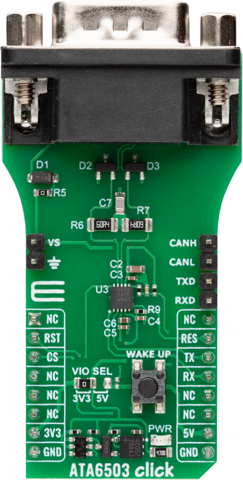
ATA6503 Click is based on the ATA6503, a fully integrated high-speed CAN FD System Basis Chip (SBC) from Microchip. This automotive-qualified device, meeting Grade 0 AEC-Q100 standards, is a reliable interface between a Controller Area Network (CAN) protocol controller and the physical two-wire CAN bus. It supports both Classical CAN and CAN FD communication protocols, achieving data rates of up to 8Mbit/s. Its differential transmit and receive capabilities simplify communication with a CAN protocol controller, enabling the development of reliable CAN nodes. Fully compliant with ISO 11898-2:2024 and SAE J2284-1 to SAE J2284-5 specifications, the ATA6503 ensures compatibility with modern automotive and industrial CAN applications like body electronics and lighting, automotive infotainment systems, powertrain systems, Advanced Driver Assistance Systems (ADAS), photovoltaic systems, and many other scenarios. The ATA6503 communicates with the host MCU through a UART interface, with a default baud rate of 115200bps. This Click board™ features a standard DB-9 connector, allowing straightforward integration with the CAN bus. For added versatility, both CAN and UART signals are accessible through additional pins on the right side of the Click board™, allowing flexible control options such as monitoring data flow, configuring
alternative communication paths, or integrating with auxiliary devices in complex systems. The high-speed CAN FD SBC ATA6503 supports multiple operating modes, advanced diagnostic features, and fail-safe mechanisms, contributing to system reliability and power management. The control pins EN (muxed with ClickID control CS pin) and TXD (connected to the RX pin on the mikroBUS™ socket) select one of the five operating modes provided by the ATA6503 to suit various application requirements. The ATA6503 includes a RES pin (open-drain reset output (active low)) designed to allow a wired-OR connection to multiple independent reset sources. Furthermore, the board also has a dedicated WAKE UP button, which enables the ATA6503 to transition out of Sleep mode. The ATA6503 also features an integrated 5V/150mA voltage regulator capable of powering the CAN FD transceiver, a 5V MCU, and other components or loads on the PCB. In cases where the entire system needs to be powered through the internal 5V regulator, the R11 resistor, left unsoldered by default, must be installed to enable this functionality. The regulator has protection mechanisms for reliable operation under varying conditions, including current limitations and overtemperature shutdown. Additionally, the output voltage is continuously monitored while the
regulator is active, and in the event of an overvoltage condition, the regulator automatically shuts down to prevent potential damage to the system. In addition to the CAN and TXD/RXD pins, the board includes a header with a VS pin, which serves as an external power supply input, supporting a voltage range from 4.5V to 28V. This pin is connected to the power source through a serial diode, providing reverse battery protection and ensuring reliable operation under standard automotive conditions. An integrated undervoltage detection circuit further enhances system reliability by preventing malfunctions or false bus messages caused by insufficient supply voltage. Upon powering the VS pin, the ATA6503 enters Reset mode, which activates the internal voltage regulator. Once the regulated voltage stabilizes, the device transitions to Standby mode, ready for further operation. This Click board™ can operate with either 3.3V or 5V logic voltage levels selected via the VIO SEL jumper. This way, both 3.3V and 5V capable MCUs can use the communication lines properly. Also, this Click board™ comes equipped with a library containing easy-to-use functions and an example code that can be used as a reference for further development.

Features overview
Development board
Clicker 2 for Kinetis is a compact starter development board that brings the flexibility of add-on Click boards™ to your favorite microcontroller, making it a perfect starter kit for implementing your ideas. It comes with an onboard 32-bit ARM Cortex-M4F microcontroller, the MK64FN1M0VDC12 from NXP Semiconductors, two mikroBUS™ sockets for Click board™ connectivity, a USB connector, LED indicators, buttons, a JTAG programmer connector, and two 26-pin headers for interfacing with external electronics. Its compact design with clear and easily recognizable silkscreen markings allows you to build gadgets with unique functionalities and
features quickly. Each part of the Clicker 2 for Kinetis development kit contains the components necessary for the most efficient operation of the same board. In addition to the possibility of choosing the Clicker 2 for Kinetis programming method, using a USB HID mikroBootloader or an external mikroProg connector for Kinetis programmer, the Clicker 2 board also includes a clean and regulated power supply module for the development kit. It provides two ways of board-powering; through the USB Micro-B cable, where onboard voltage regulators provide the appropriate voltage levels to each component on the board, or
using a Li-Polymer battery via an onboard battery connector. All communication methods that mikroBUS™ itself supports are on this board, including the well-established mikroBUS™ socket, reset button, and several user-configurable buttons and LED indicators. Clicker 2 for Kinetis is an integral part of the Mikroe ecosystem, allowing you to create a new application in minutes. Natively supported by Mikroe software tools, it covers many aspects of prototyping thanks to a considerable number of different Click boards™ (over a thousand boards), the number of which is growing every day.

Microcontroller Overview
MCU Card / MCU

Architecture
ARM Cortex-M4
MCU Memory (KB)
1024
Silicon Vendor
NXP
Pin count
121
RAM (Bytes)
262144
You complete me!
Accessories
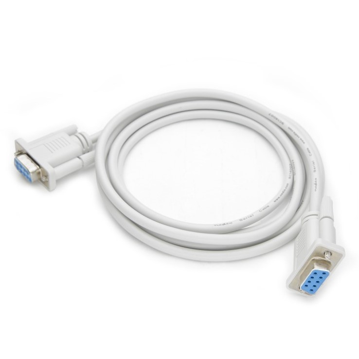
DB9 Cable Female-to-Female (2m) cable is essential for establishing dependable serial data connections between devices. With its DB9 female connectors on both ends, this cable enables a seamless link between various equipment, such as computers, routers, switches, and other serial devices. Measuring 2 meters in length, it offers flexibility in arranging your setup without compromising data transmission quality. Crafted with precision, this cable ensures consistent and reliable data exchange, making it suitable for industrial applications, office environments, and home setups. Whether configuring networking equipment, accessing console ports, or utilizing serial peripherals, this cable's durable construction and robust connectors guarantee a stable connection. Simplify your data communication needs with the 2m DB9 female-to-female cable, an efficient solution designed to meet your serial connectivity requirements easily and efficiently.
Used MCU Pins
mikroBUS™ mapper
Take a closer look
Click board™ Schematic

Step by step
Project assembly

Start by selecting your development board and Click board™. Begin with the Clicker 2 for Kinetis as your development board.


Track your results in real time
Application Output
1. Application Output - In Debug mode, the 'Application Output' window enables real-time data monitoring, offering direct insight into execution results. Ensure proper data display by configuring the environment correctly using the provided tutorial.

2. UART Terminal - Use the UART Terminal to monitor data transmission via a USB to UART converter, allowing direct communication between the Click board™ and your development system. Configure the baud rate and other serial settings according to your project's requirements to ensure proper functionality. For step-by-step setup instructions, refer to the provided tutorial.

3. Plot Output - The Plot feature offers a powerful way to visualize real-time sensor data, enabling trend analysis, debugging, and comparison of multiple data points. To set it up correctly, follow the provided tutorial, which includes a step-by-step example of using the Plot feature to display Click board™ readings. To use the Plot feature in your code, use the function: plot(*insert_graph_name*, variable_name);. This is a general format, and it is up to the user to replace 'insert_graph_name' with the actual graph name and 'variable_name' with the parameter to be displayed.

Software Support
Library Description
ATA6503 Click demo application is developed using the NECTO Studio, ensuring compatibility with mikroSDK's open-source libraries and tools. Designed for plug-and-play implementation and testing, the demo is fully compatible with all development, starter, and mikromedia boards featuring a mikroBUS™ socket.
Example Description
This example demonstrates the use of an ATA6503 Click board by showing the communication between the two Click boards.
Key functions:
ata6503_cfg_setup- Config Object Initialization function.ata6503_init- Initialization function.ata6503_generic_write- This function writes a desired number of data bytes by using UART serial interface.ata6503_generic_read- This function reads a desired number of data bytes by using UART serial interface.ata6503_set_en_pin- This function sets the EN pin logic state.
Application Init
Initializes the driver and logger.
Application Task
Depending on the selected application mode, it reads all the received data or sends the desired message every 3 seconds.
Open Source
Code example
The complete application code and a ready-to-use project are available through the NECTO Studio Package Manager for direct installation in the NECTO Studio. The application code can also be found on the MIKROE GitHub account.
/*!
 * @file main.c
 * @brief ATA6503 Click Example.
 *
 * # Description
 * This example demonstrates the use of an ATA6503 Click board by showing
 * the communication between the two Click boards.
 *
 * The demo application is composed of two sections :
 *
 * ## Application Init
 * Initializes the driver and logger.
 *
 * ## Application Task
 * Depending on the selected application mode, it reads all the received data or
 * sends the desired message every 3 seconds.
 *
 * ## Additional Function
 * - static void ata6503_clear_app_buf ( void )
 * - static void ata6503_log_app_buf ( void )
 * - static err_t ata6503_process ( ata6503_t *ctx )
 *
 * @author Stefan Filipovic
 *
 */

#include "board.h"
#include "log.h"
#include "ata6503.h"

// Comment out the line below in order to switch the application mode to receiver
#define DEMO_APP_TRANSMITTER

// Text message to send in the transmitter application mode
#define DEMO_TEXT_MESSAGE           "MIKROE - ATA6503 Click board\r\n"

// Application buffer size
#define APP_BUFFER_SIZE             500
#define PROCESS_BUFFER_SIZE         200

static ata6503_t ata6503;
static log_t logger;

static uint8_t app_buf[ APP_BUFFER_SIZE ] = { 0 };
static int32_t app_buf_len = 0;

/**
 * @brief ATA6503 clearing application buffer.
 * @details This function clears memory of application buffer and reset its length.
 * @note None.
 */
static void ata6503_clear_app_buf ( void );

/**
 * @brief ATA6503 log application buffer.
 * @details This function logs data from application buffer to USB UART.
 * @note None.
 */
static void ata6503_log_app_buf ( void );

/**
 * @brief ATA6503 data reading function.
 * @details This function reads data from device and concatenates data to application buffer.
 * @param[in] ctx : Click context object.
 * See #ata6503_t object definition for detailed explanation.
 * @return @li @c  0 - Read some data.
 *         @li @c -1 - Nothing is read.
 * See #err_t definition for detailed explanation.
 * @note None.
 */
static err_t ata6503_process ( ata6503_t *ctx );

void application_init ( void )
{
    log_cfg_t log_cfg;  /**< Logger config object. */
    ata6503_cfg_t ata6503_cfg;  /**< Click config object. */

    /**
     * Logger initialization.
     * Default baud rate: 115200
     * Default log level: LOG_LEVEL_DEBUG
     * @note If USB_UART_RX and USB_UART_TX
     * are defined as HAL_PIN_NC, you will
     * need to define them manually for log to work.
     * See @b LOG_MAP_USB_UART macro definition for detailed explanation.
     */
    LOG_MAP_USB_UART( log_cfg );
    log_init( &logger, &log_cfg );
    log_info( &logger, " Application Init " );

    // Click initialization.
    ata6503_cfg_setup( &ata6503_cfg );
    ATA6503_MAP_MIKROBUS( ata6503_cfg, MIKROBUS_1 );
    if ( UART_ERROR == ata6503_init( &ata6503, &ata6503_cfg ) )
    {
        log_error( &logger, " Communication init." );
        for ( ; ; );
    }

#ifdef DEMO_APP_TRANSMITTER
    log_printf( &logger, " Application Mode: Transmitter\r\n" );
#else
    log_printf( &logger, " Application Mode: Receiver\r\n" );
#endif

    log_info( &logger, " Application Task " );
}

void application_task ( void )
{
#ifdef DEMO_APP_TRANSMITTER
    ata6503_generic_write( &ata6503, DEMO_TEXT_MESSAGE, strlen( DEMO_TEXT_MESSAGE ) );
    log_printf( &logger, "%s", ( char * ) DEMO_TEXT_MESSAGE );
    Delay_ms ( 1000 );
    Delay_ms ( 1000 );
    Delay_ms ( 1000 );
#else
    if ( ATA6503_OK == ata6503_process( &ata6503 ) )
    {
        ata6503_log_app_buf ( );
        ata6503_clear_app_buf ( );
    }
#endif
}

int main ( void )
{
    /* Do not remove this line or clock might not be set correctly. */
    #ifdef PREINIT_SUPPORTED
    preinit();
    #endif

    application_init( );

    for ( ; ; )
    {
        application_task( );
    }

    return 0;
}

static void ata6503_clear_app_buf ( void )
{
    memset( app_buf, 0, app_buf_len );
    app_buf_len = 0;
}

static void ata6503_log_app_buf ( void )
{
    for ( int32_t buf_cnt = 0; buf_cnt < app_buf_len; buf_cnt++ )
    {
        log_printf( &logger, "%c", app_buf[ buf_cnt ] );
    }
}

static err_t ata6503_process ( ata6503_t *ctx )
{
    uint8_t rx_buf[ PROCESS_BUFFER_SIZE ] = { 0 };
    int32_t overflow_bytes = 0;
    int32_t rx_cnt = 0;
    int32_t rx_size = ata6503_generic_read( ctx, rx_buf, PROCESS_BUFFER_SIZE );
    if ( ( rx_size > 0 ) && ( rx_size <= APP_BUFFER_SIZE ) )
    {
        if ( ( app_buf_len + rx_size ) > APP_BUFFER_SIZE )
        {
            overflow_bytes = ( app_buf_len + rx_size ) - APP_BUFFER_SIZE;
            app_buf_len = APP_BUFFER_SIZE - rx_size;
            memmove ( app_buf, &app_buf[ overflow_bytes ], app_buf_len );
            memset ( &app_buf[ app_buf_len ], 0, overflow_bytes );
        }
        for ( rx_cnt = 0; rx_cnt < rx_size; rx_cnt++ )
        {
            if ( rx_buf[ rx_cnt ] )
            {
                app_buf[ app_buf_len++ ] = rx_buf[ rx_cnt ];
            }
        }
        return ATA6503_OK;
    }
    return ATA6503_ERROR;
}

// ------------------------------------------------------------------------ END


