Be the best in high-speed CAN industrial applications with ATA6570 and STM32F446RE
Embrace the future with CAN technology

Published Oct 08, 2024
Click board™
ATA6570 Click
Dev. board
Nucleo 64 with STM32F446RE MCU
Compiler
NECTO Studio
MCU
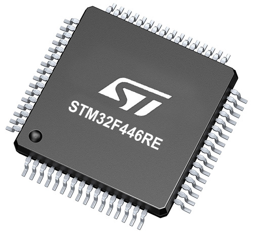
STM32F446RE
Empower high-speed data exchange with our advanced CAN transceiver, revolutionizing automotive communication
A
A
Hardware Overview
How does it work?
ATA6570 Click uses the ATA6570, a standalone high-speed CAN transceiver IC from Microchip, with partial networking support. This IC supports CAN and recently established CAN FD protocols, up to 1Mbit/s and 5Mbit/s, respectively. The communication inside the CAN bus is differential and performed through the twisted pairs with the characteristic impedance of 120Ω. The CANH and CANL drivers drive the differential lines. This provides robustness and immunity to electromagnetic interferences, typically observed in automotive systems. The ISO 11898 standard defines a signal line of twisted-pair cable as the network topology, terminated by the resistors with the characteristic impedance of the CAN bus (120Ω) at both ends - to prevent signal reflection. The dominant/recessive states are used for the message priority arbitration - the node which transmits the signal with the higher priority (the lower the binary message identifier number, the higher the priority) will win the arbitration, and the node with the lower priority will abort the transmission, waiting for the bus to become available again. Since the high logic level on the CAN line is considered recessive, the TXD line has an internal pull-up resistor, making the ATA6570 device stay recessive if the pin is left floating. The ATA6570 device can be driven in the recessive or dominant state with the TXD pin: when the TXD pin is at the VCC level and works in Normal mode, the drivers at the CANH and CANL pins are turned off. These pins are biased at 2.5 (VCC/2), with respect to the GND, provided by the internal autonomous bus biasing circuitry, and the CAN driver is in a recessive state. Pulling the TXD pin to the GND will activate the CANH and CANL drivers and set the bus to the dominant state.
A TXD dominant timeout timer is started when the TXD pin is set to low. If the low state on the TXD pin persists for longer than the predetermined time, the transmitter will be disabled, releasing the bus lines to the recessive state. This function prevents the hardware or software failure from driving the bus lines to a permanent dominant state, blocking all network communications. When the device is in the Sleep or Unpowered mode, the drivers will become highly resistive, rendering the device passive and completely ignored by the CAN bus network. Although the RXD and TXD lines are interfaced with the microcontroller, the SPI bus sets the internal registers, such as the partial networking registers and other status and configuration-related registers. The provided MikroElektronika library contains functions to easily set the parameters via the SPI bus and establish communication with the nodes. Partial networking allows selective wake-up of ATA6570 Click. Dedicated predefined frames can wake the device if configured to accept these frames. For this reason, when the device is in Standby or Sleep mode, it will still actively monitor the bus for those frames. SPI can set the wake-up CAN frame ID and data. Besides waking up the device by the partial networking feature, the device can also be woken up by a remote wake-up pattern on the CAN bus or with the onboard switch connected to the WAKE pin of the ATA6570 IC. Another wake-up source can be the SPI command for those modes where the SPI module is active and the remote wake-up pattern on the CAN bus. When in Sleep, MCU Reset or Power Off mode, the INH pin, which is routed to the external regulators, will be turned off, reducing the power consumption of the
external elements. The #SHDN (shutdown) pins of the two LDO regulators found on the ATA6570 Click are connected to the INH pin. Both regulators take power from the car battery connector (VS pin), providing 5V and 3.3V for custom needs. Outputs of those LDOs are routed via the SMD jumpers that can be populated so that the LDOs can be used to power up the mikroBUS™ 3.3V and 5V power rails. However, it should be noted that MikroElektronika does not advise powering up its systems this way - that is why these jumpers are left unpopulated by default. Overtemperature mode is activated when the device's temperature becomes too high, and the device was previously working in Normal mode. The ATA6570 provides two levels of overtemperature protection. When the first temperature level threshold is reached, an alarm is in the form of an interrupt on the RX pin (if set) and an appropriate status bit. If the temperature rises, the device will shut down the CAN drivers. Microcontroller Reset mode utilizes an integrated watchdog. When the watchdog event occurs, it will trigger a pulse on the INH pin - this pin will be turned off for a predetermined period, performing a power cycle reset on all devices connected via the ATA6570 click LDOs. This is a power cycle reset measure for a custom system powered via the mikroBUS™ socket. The onboard SMD jumper labeled as the VIO SEL selects which voltage rail of two LDO regulators will be used as the logic voltage level (SPI, UART). It offers voltage selection between 3.3V and 5V so that the click board™ can be interfaced with both the 3.3V and 5V capable MCUs.

Features overview
Development board
Nucleo-64 with STM32F446RE MCU offers a cost-effective and adaptable platform for developers to explore new ideas and prototype their designs. This board harnesses the versatility of the STM32 microcontroller, enabling users to select the optimal balance of performance and power consumption for their projects. It accommodates the STM32 microcontroller in the LQFP64 package and includes essential components such as a user LED, which doubles as an ARDUINO® signal, alongside user and reset push-buttons, and a 32.768kHz crystal oscillator for precise timing operations. Designed with expansion and flexibility in mind, the Nucleo-64 board features an ARDUINO® Uno V3 expansion connector and ST morpho extension pin
headers, granting complete access to the STM32's I/Os for comprehensive project integration. Power supply options are adaptable, supporting ST-LINK USB VBUS or external power sources, ensuring adaptability in various development environments. The board also has an on-board ST-LINK debugger/programmer with USB re-enumeration capability, simplifying the programming and debugging process. Moreover, the board is designed to simplify advanced development with its external SMPS for efficient Vcore logic supply, support for USB Device full speed or USB SNK/UFP full speed, and built-in cryptographic features, enhancing both the power efficiency and security of projects. Additional connectivity is
provided through dedicated connectors for external SMPS experimentation, a USB connector for the ST-LINK, and a MIPI® debug connector, expanding the possibilities for hardware interfacing and experimentation. Developers will find extensive support through comprehensive free software libraries and examples, courtesy of the STM32Cube MCU Package. This, combined with compatibility with a wide array of Integrated Development Environments (IDEs), including IAR Embedded Workbench®, MDK-ARM, and STM32CubeIDE, ensures a smooth and efficient development experience, allowing users to fully leverage the capabilities of the Nucleo-64 board in their projects.

Microcontroller Overview
MCU Card / MCU
Architecture
ARM Cortex-M4
MCU Memory (KB)
512
Silicon Vendor
STMicroelectronics
Pin count
64
RAM (Bytes)
131072
You complete me!
Accessories
Click Shield for Nucleo-64 comes equipped with two proprietary mikroBUS™ sockets, allowing all the Click board™ devices to be interfaced with the STM32 Nucleo-64 board with no effort. This way, Mikroe allows its users to add any functionality from our ever-growing range of Click boards™, such as WiFi, GSM, GPS, Bluetooth, ZigBee, environmental sensors, LEDs, speech recognition, motor control, movement sensors, and many more. More than 1537 Click boards™, which can be stacked and integrated, are at your disposal. The STM32 Nucleo-64 boards are based on the microcontrollers in 64-pin packages, a 32-bit MCU with an ARM Cortex M4 processor operating at 84MHz, 512Kb Flash, and 96KB SRAM, divided into two regions where the top section represents the ST-Link/V2 debugger and programmer while the bottom section of the board is an actual development board. These boards are controlled and powered conveniently through a USB connection to program and efficiently debug the Nucleo-64 board out of the box, with an additional USB cable connected to the USB mini port on the board. Most of the STM32 microcontroller pins are brought to the IO pins on the left and right edge of the board, which are then connected to two existing mikroBUS™ sockets. This Click Shield also has several switches that perform functions such as selecting the logic levels of analog signals on mikroBUS™ sockets and selecting logic voltage levels of the mikroBUS™ sockets themselves. Besides, the user is offered the possibility of using any Click board™ with the help of existing bidirectional level-shifting voltage translators, regardless of whether the Click board™ operates at a 3.3V or 5V logic voltage level. Once you connect the STM32 Nucleo-64 board with our Click Shield for Nucleo-64, you can access hundreds of Click boards™, working with 3.3V or 5V logic voltage levels.

DB9 Cable Female-to-Female (2m) cable is essential for establishing dependable serial data connections between devices. With its DB9 female connectors on both ends, this cable enables a seamless link between various equipment, such as computers, routers, switches, and other serial devices. Measuring 2 meters in length, it offers flexibility in arranging your setup without compromising data transmission quality. Crafted with precision, this cable ensures consistent and reliable data exchange, making it suitable for industrial applications, office environments, and home setups. Whether configuring networking equipment, accessing console ports, or utilizing serial peripherals, this cable's durable construction and robust connectors guarantee a stable connection. Simplify your data communication needs with the 2m DB9 female-to-female cable, an efficient solution designed to meet your serial connectivity requirements easily and efficiently.

Used MCU Pins
mikroBUS™ mapper
Take a closer look
Click board™ Schematic

Step by step
Project assembly
Start by selecting your development board and Click board™. Begin with the Nucleo 64 with STM32F446RE MCU as your development board.


Track your results in real time
Application Output
1. Application Output - In Debug mode, the 'Application Output' window enables real-time data monitoring, offering direct insight into execution results. Ensure proper data display by configuring the environment correctly using the provided tutorial.

2. UART Terminal - Use the UART Terminal to monitor data transmission via a USB to UART converter, allowing direct communication between the Click board™ and your development system. Configure the baud rate and other serial settings according to your project's requirements to ensure proper functionality. For step-by-step setup instructions, refer to the provided tutorial.

3. Plot Output - The Plot feature offers a powerful way to visualize real-time sensor data, enabling trend analysis, debugging, and comparison of multiple data points. To set it up correctly, follow the provided tutorial, which includes a step-by-step example of using the Plot feature to display Click board™ readings. To use the Plot feature in your code, use the function: plot(*insert_graph_name*, variable_name);. This is a general format, and it is up to the user to replace 'insert_graph_name' with the actual graph name and 'variable_name' with the parameter to be displayed.

Software Support
Library Description
This library contains API for ATA6570 Click driver.
Key functions:
ata6570_write_reg- Write Registerata6570_read_reg- Read Register
Open Source
Code example
The complete application code and a ready-to-use project are available through the NECTO Studio Package Manager for direct installation in the NECTO Studio. The application code can also be found on the MIKROE GitHub account.
/*!
 * \file
 * \brief Ata6570 Click example
 *
 * # Description
 * This application is interfaces a Controller Area Network (CAN) protocol controller and the physical two-wire CAN bus.
 *
 * The demo application is composed of two sections :
 *
 * ## Application Init
 * In addition to this module is palced inside normal working mode cappable of tranmission and reception of data.
 *
 * ## Application Task
 * Tranismiter/Receiver task depend on uncommented code
  Receiver logging each received byte to the UART for data logging, while transmiter send message each
  2 seconds.
 *
 *
 * \author MikroE Team
 *
 */
// ------------------------------------------------------------------- INCLUDES

#include "board.h"
#include "log.h"
#include "ata6570.h"


// ------------------------------------------------------------------ VARIABLES

#define PROCESS_RX_BUFFER_SIZE 500

// #define DEMO_APP_RECEIVER
#define DEMO_APP_TRANSMITER

static ata6570_t ata6570;
static log_t logger;

static char demo_message[ 9 ] = { 'M', 'i', 'k', 'r', 'o', 'E', 13, 10, 0 };
static int32_t rsp_size;
static char uart_rx_buffer[ PROCESS_RX_BUFFER_SIZE ] = { 0 };

// ------------------------------------------------------ APPLICATION FUNCTIONS

void application_init ( void )
{
    log_cfg_t log_cfg;
    ata6570_cfg_t cfg;

    /**
     * Logger initialization.
     * Default baud rate: 115200
     * Default log level: LOG_LEVEL_DEBUG
     * @note If USB_UART_RX and USB_UART_TX
     * are defined as HAL_PIN_NC, you will
     * need to define them manually for log to work.
     * See @b LOG_MAP_USB_UART macro definition for detailed explanation.
     */
    LOG_MAP_USB_UART( log_cfg );
    log_init( &logger, &log_cfg );
    log_info( &logger, "---- Application Init ----" );

    //  Click initialization.

    ata6570_cfg_setup( &cfg );
    ATA6570_MAP_MIKROBUS( cfg, MIKROBUS_1 );
    ata6570_init( &ata6570, &cfg );
    ata6570_write_reg( &ata6570, ATA6570_DMCR, ATA6570_OPMODE_NORMAL );
    Delay_ms ( 500 );
}

void application_task ( void )
{
    //  Task implementation.

#ifdef DEMO_APP_RECEIVER
       // RECEIVER - UART polling
      rsp_size = ata6570_generic_read( &ata6570, uart_rx_buffer, PROCESS_RX_BUFFER_SIZE );

      if ( rsp_size > 0 )
        {
            log_printf( &logger, "%s", uart_rx_buffer );
            memset( uart_rx_buffer, 0, rsp_size );
        }
#endif

#ifdef DEMO_APP_TRANSMITER
       // TRANSMITER - TX each 2 sec
       for( uint8_t i = 0; i < 8; i++ )
       {
           ata6570_generic_write( &ata6570, &demo_message[ i ], 1 );
       }
       Delay_ms ( 1000 );
       Delay_ms ( 1000 );
#endif
}

int main ( void )
{
    /* Do not remove this line or clock might not be set correctly. */
    #ifdef PREINIT_SUPPORTED
    preinit();
    #endif

    application_init( );

    for ( ; ; )
    {
        application_task( );
    }

    return 0;
}

// ------------------------------------------------------------------------ END


