The best available custom ADC solution with ADS131M02 and TM4C1299NCZAD
Go digital with ADC!

Published Jun 01, 2023
Click board™
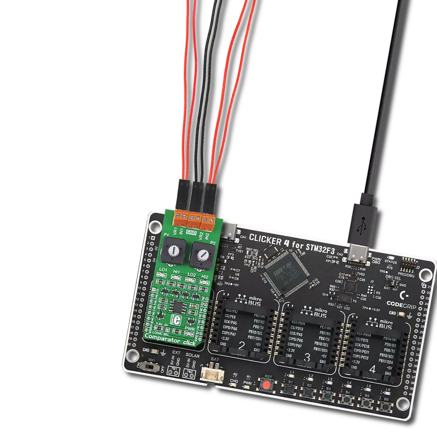
ADC 15 Click
Dev. board
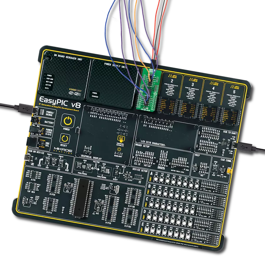
Fusion for Tiva v8
Compiler
NECTO Studio
MCU
TM4C1299NCZAD
Discover what our advanced ADC can do for your engineering solutions – check it out now!
A
A
Hardware Overview
How does it work?
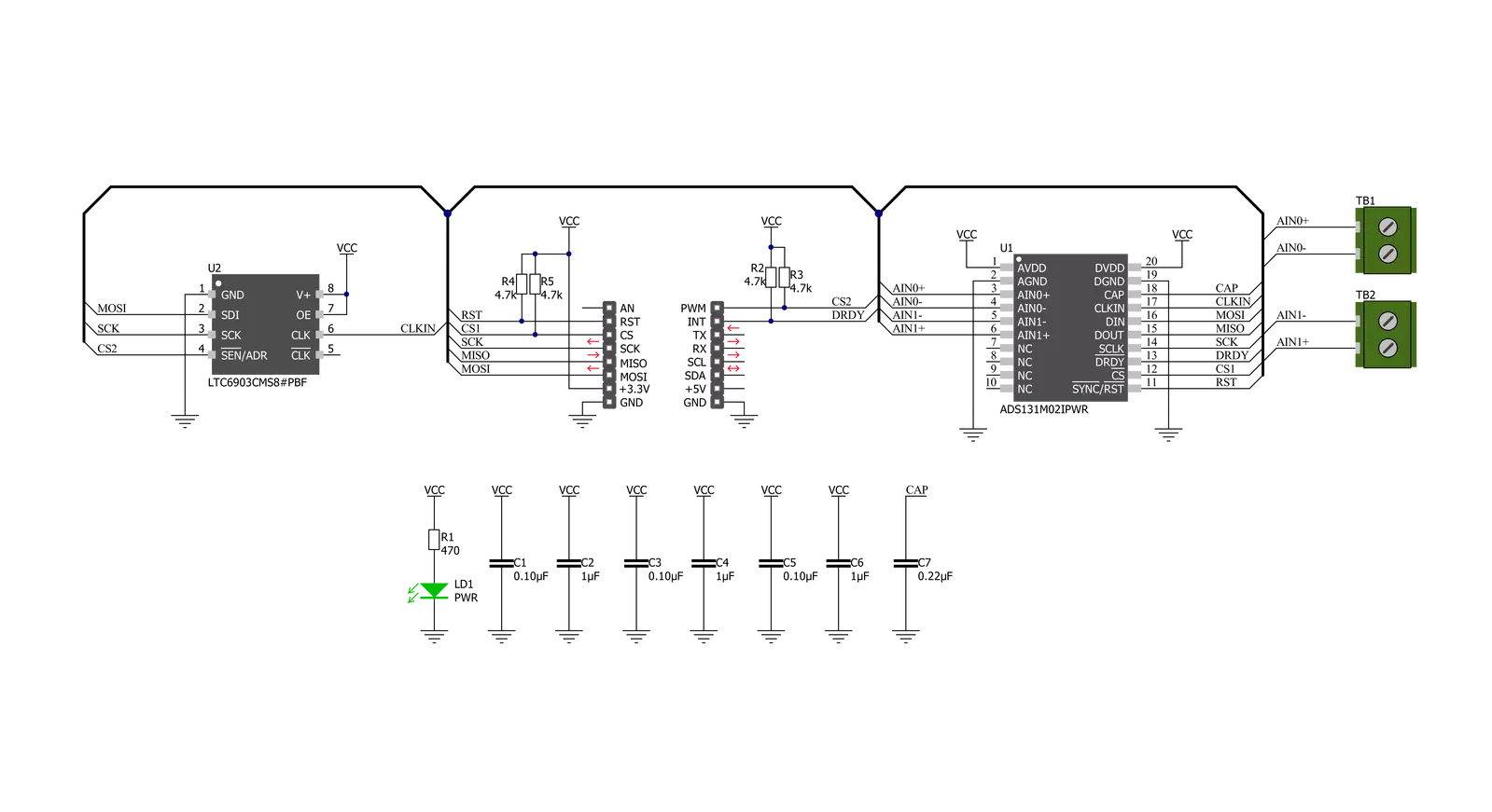
ADC 15 Click is based on the ADS131M02, a low-power, two-channel, simultaneously sampling, 24-bit, delta-sigma (ΔΣ) analog-to-digital converter (ADC) with a low-drift internal reference voltage from Texas Instruments. The dynamic range, size, feature set, and power consumption are optimized for cost-sensitive applications requiring simultaneous sampling. An integrated negative charge pump allows absolute input voltages as low as -1.3V, enabling input signal measurements varying around the ground with a single-ended power supply. The ADS131M02 features a programmable gain amplifier (PGA) with gains up to 128. An integrated input pre-charge buffer enabled at gains greater than 4 ensures high input impedance at high PGA gain settings. The ADC receives its reference voltage from an integrated 1.2V reference, allowing differential input voltages as large as the reference. Each channel on the ADS131M02 contains a digital
decimation filter that demodulates the output of the ΔΣ modulators. The filter enables data rates as high as 32kSPS per channel in high-resolution mode. The relative phase of the samples can be configured between channels, thus allowing an accurate compensation for the sensor phase response. Offset and gain calibration registers can be programmed to automatically adjust output samples for measured offset and gain errors. The ADC 15 Click communicates with MCU through a standard SPI interface to read the conversion data and configure and control the ADS131M02, supporting the most common SPI mode - SPI Mode 1. To normally run the ADS131M02, an LVCMOS clock must be continuously provided at the CLKIN pin, which is achieved with the LTC6903 programmable oscillator activated via the CS2 pin routed to the PWM pin on the mikroBUS™ socket. The frequency of the clock can be scaled in conjunction
with the power mode to provide a trade-off between power consumption and dynamic range. Selection of the bits in the CLOCK register allows the device to be configured in one of three power modes: high-resolution (HR) mode, low-power (LP) mode, and very low-power (VLP) mode. In addition, this Click board™ also uses features such as data-ready/interrupt routed to the INT pin on the mikroBUS™ socket, which serves as a flag to the host to indicate that new conversion data are available and Reset routed to the RST pin that allows for a hardware device reset. This Click board™ can only be operated with a 3.3V logic voltage level. The board must perform appropriate logic voltage level conversion before using MCUs with different logic levels. However, the Click board™ comes equipped with a library containing functions and an example code that can be used as a reference for further development.


Features overview
Development board
Fusion for TIVA v8 is a development board specially designed for the needs of rapid development of embedded applications. It supports a wide range of microcontrollers, such as different 32-bit ARM® Cortex®-M based MCUs from Texas Instruments, regardless of their number of pins, and a broad set of unique functions, such as the first-ever embedded debugger/programmer over a WiFi network. The development board is well organized and designed so that the end-user has all the necessary elements, such as switches, buttons, indicators, connectors, and others, in one place. Thanks to innovative manufacturing technology, Fusion for TIVA v8 provides a fluid and immersive working experience, allowing access
anywhere and under any circumstances at any time. Each part of the Fusion for TIVA v8 development board contains the components necessary for the most efficient operation of the same board. An advanced integrated CODEGRIP programmer/debugger module offers many valuable programming/debugging options, including support for JTAG, SWD, and SWO Trace (Single Wire Output)), and seamless integration with the Mikroe software environment. Besides, it also includes a clean and regulated power supply module for the development board. It can use a wide range of external power sources, including a battery, an external 12V power supply, and a power source via the USB Type-C (USB-C) connector.
Communication options such as USB-UART, USB HOST/DEVICE, CAN (on the MCU card, if supported), and Ethernet is also included. In addition, it also has the well-established mikroBUS™ standard, a standardized socket for the MCU card (SiBRAIN standard), and two display options for the TFT board line of products and character-based LCD. Fusion for TIVA v8 is an integral part of the Mikroe ecosystem for rapid development. Natively supported by Mikroe software tools, it covers many aspects of prototyping and development thanks to a considerable number of different Click boards™ (over a thousand boards), the number of which is growing every day.

Microcontroller Overview
MCU Card / MCU
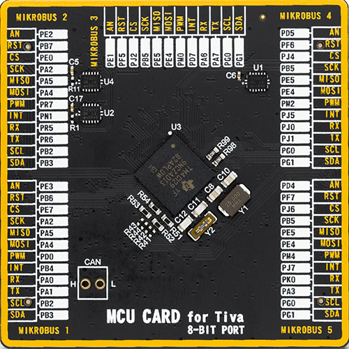
Type
8th Generation
Architecture
ARM Cortex-M4
MCU Memory (KB)
1024
Silicon Vendor
Texas Instruments
Pin count
212
RAM (Bytes)
262144
Used MCU Pins
mikroBUS™ mapper
Take a closer look
Click board™ Schematic
Step by step
Project assembly

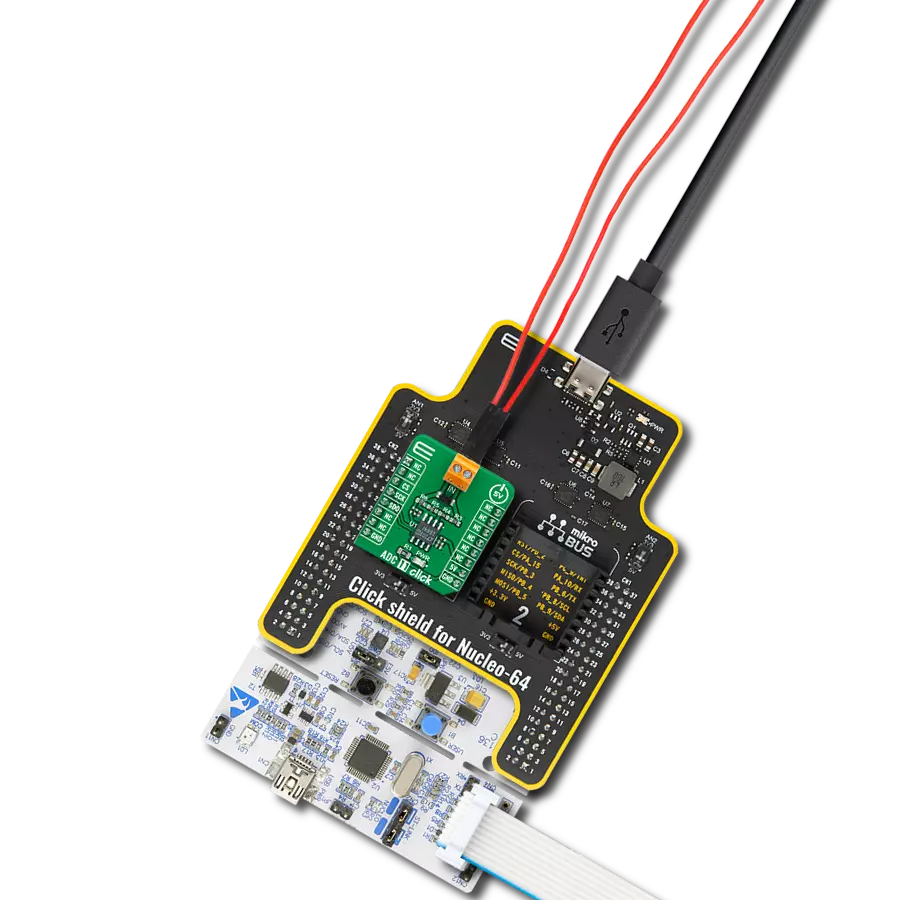
Start by selecting your development board and Click board™. Begin with the Fusion for Tiva v8 as your development board.


Track your results in real time
Application Output
1. Application Output - In Debug mode, the 'Application Output' window enables real-time data monitoring, offering direct insight into execution results. Ensure proper data display by configuring the environment correctly using the provided tutorial.

2. UART Terminal - Use the UART Terminal to monitor data transmission via a USB to UART converter, allowing direct communication between the Click board™ and your development system. Configure the baud rate and other serial settings according to your project's requirements to ensure proper functionality. For step-by-step setup instructions, refer to the provided tutorial.

3. Plot Output - The Plot feature offers a powerful way to visualize real-time sensor data, enabling trend analysis, debugging, and comparison of multiple data points. To set it up correctly, follow the provided tutorial, which includes a step-by-step example of using the Plot feature to display Click board™ readings. To use the Plot feature in your code, use the function: plot(*insert_graph_name*, variable_name);. This is a general format, and it is up to the user to replace 'insert_graph_name' with the actual graph name and 'variable_name' with the parameter to be displayed.

Software Support
Library Description
This library contains API for ADC 15 Click driver.
Key functions:
adc15_read_voltageGet voltage value.adc15_set_gainSet gain for channel.adc15_set_word_lenSet word len.
Open Source
Code example
The complete application code and a ready-to-use project are available through the NECTO Studio Package Manager for direct installation in the NECTO Studio. The application code can also be found on the MIKROE GitHub account.
/*!
* @file main.c
* @brief ADC15 Click example
*
* # Description
* This example showcases ability of the Click board to
* read adc data from 2 different channels. It's also configuratable
* to read data in different output rate, resolutions( word/data len ),
* and gain.
*
* The demo application is composed of two sections :
*
* ## Application Init
* Initialization of communication modules (SPI, UART) and additional
* pins for control of the device. Sets default configuration, that
* sets gain of 1 for both channels(+/-1.2V range) and word/data length
* of 24bit. In the end reads device ID.
*
* ## Application Task
* Waits for data ready signal and reads voltage value of both channels,
* and logs read status and channel voltage level.
*
* @author Luka Filipovic
*
*/
#include "board.h"
#include "log.h"
#include "adc15.h"
#include "math.h"
static adc15_t adc15;
static log_t logger;
void application_init ( void )
{
log_cfg_t log_cfg; /**< Logger config object. */
adc15_cfg_t adc15_cfg; /**< Click config object. */
/**
* Logger initialization.
* Default baud rate: 115200
* Default log level: LOG_LEVEL_DEBUG
* @note If USB_UART_RX and USB_UART_TX
* are defined as HAL_PIN_NC, you will
* need to define them manually for log to work.
* See @b LOG_MAP_USB_UART macro definition for detailed explanation.
*/
LOG_MAP_USB_UART( log_cfg );
log_init( &logger, &log_cfg );
log_info( &logger, " Application Init " );
// Click initialization.
adc15_cfg_setup( &adc15_cfg );
ADC15_MAP_MIKROBUS( adc15_cfg, MIKROBUS_1 );
err_t init_flag = adc15_init( &adc15, &adc15_cfg );
if ( SPI_MASTER_ERROR == init_flag )
{
log_error( &logger, " Communication Init. " );
log_info( &logger, " Please, run program again... " );
for ( ; ; );
}
if ( adc15_default_cfg ( &adc15 ) )
{
log_error( &logger, " Default configuration. " );
for( ; ; );
}
uint16_t reg_val;
adc15_reg_read( &adc15, ADC15_REG_ID, ®_val );
log_printf( &logger, " > ID: 0x%.4X\r\n", reg_val );
log_info( &logger, " Application Task " );
Delay_ms ( 1000 );
}
void application_task ( void )
{
while ( adc15_data_ready( &adc15 ) );
float channel1 = 0;
float channel2 = 0;
uint16_t status = 0;
if ( !adc15_read_voltage( &adc15, &status, &channel1, &channel2 ) )
{
log_printf( &logger, " > Status: 0x%.4X\r\n", status );
log_printf( &logger, " > V ch1: %.3f\r\n", channel1 );
log_printf( &logger, " > V ch2: %.3f\r\n", channel2 );
log_printf( &logger, "************************\r\n" );
Delay_ms ( 1000 );
}
}
int main ( void )
{
/* Do not remove this line or clock might not be set correctly. */
#ifdef PREINIT_SUPPORTED
preinit();
#endif
application_init( );
for ( ; ; )
{
application_task( );
}
return 0;
}
// ------------------------------------------------------------------------ END