Transform your power with MIC2606 and TM4C123GH6PZ
Boost your performance!

Published Jul 26, 2023
Click board™
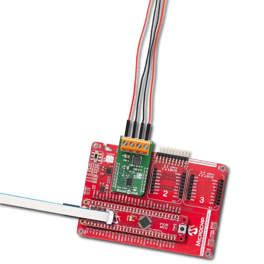
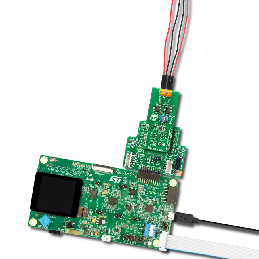
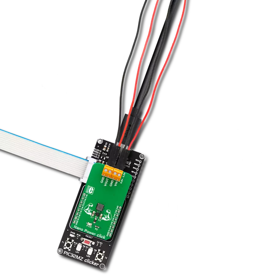
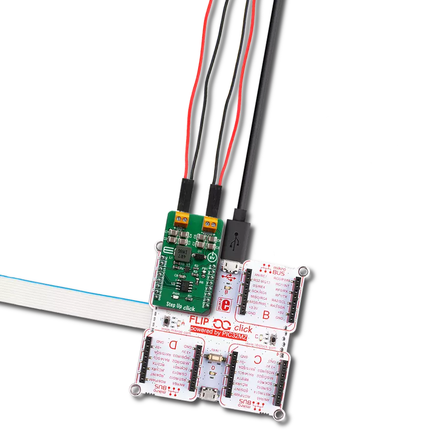
Boost Click
Dev. board
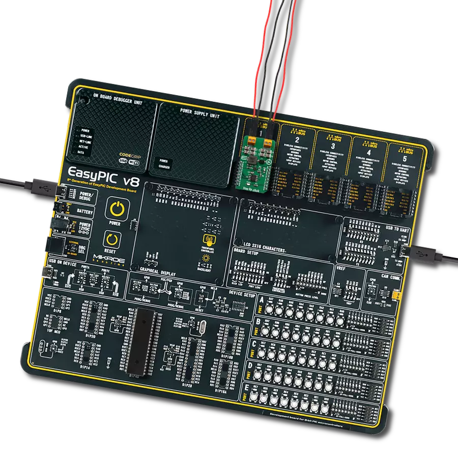
Fusion for ARM v8
Compiler
NECTO Studio
MCU
TM4C123GH6PZ
Unlock the full potential of your following projects with our voltage-booster solution
A
A
Hardware Overview
How does it work?
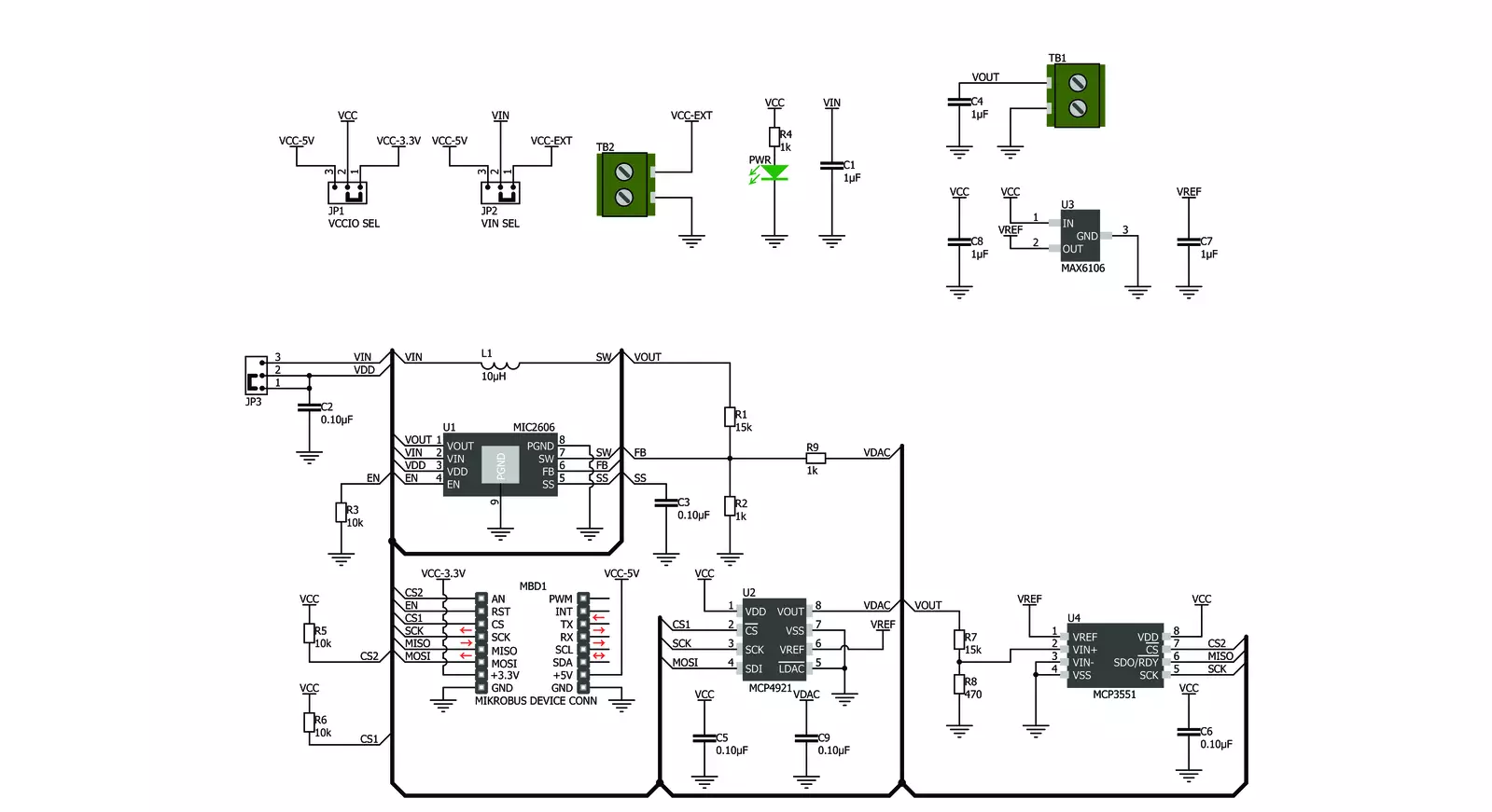
Boost Click is based on the MIC2606, a 0.5A, 2MHz wide input range boost regulator with an integrated switch and Schottky diode from Microchip. Its FB (feedback) pin provides the control path to control the output. This FB pin is driven by an onboard DAC – MCP4921. This is a 2.7 – 5.5V, low-power, low DNL, 12-Bit Digital-to-Analog Converter (DAC) with an SPI interface. It provides high accuracy and low noise performance for
industrial applications. The output voltage is connected to an onboard ADC, the MCP3551, a 2.7V to 5.5V low-power, 22-bit delta-sigma analog-to-digital converter, through a voltage divider. The input voltage can be set to 5V from mikroBUS™ or 7-20V from an external DC source connected to the VIN screw terminal. The output voltage can be set up to 38V. The reference voltage for both the ADC and DAC is provided by MAX6106 – onboard
voltage reference. This Click board™ can operate with either 3.3V or 5V logic voltage levels selected via the VCCIO SEL jumper. This way, both 3.3V and 5V capable MCUs can use the communication lines properly. However, the Click board™ comes equipped with a library containing easy-to-use functions and an example code that can be used, as a reference, for further development.

Features overview
Development board
Fusion for ARM v8 is a development board specially designed for the needs of rapid development of embedded applications. It supports a wide range of microcontrollers, such as different ARM® Cortex®-M based MCUs regardless of their number of pins, and a broad set of unique functions, such as the first-ever embedded debugger/programmer over WiFi. The development board is well organized and designed so that the end-user has all the necessary elements, such as switches, buttons, indicators, connectors, and others, in one place. Thanks to innovative manufacturing technology, Fusion for ARM v8 provides a fluid and immersive working experience, allowing access anywhere and under any
circumstances at any time. Each part of the Fusion for ARM v8 development board contains the components necessary for the most efficient operation of the same board. An advanced integrated CODEGRIP programmer/debugger module offers many valuable programming/debugging options, including support for JTAG, SWD, and SWO Trace (Single Wire Output)), and seamless integration with the Mikroe software environment. Besides, it also includes a clean and regulated power supply module for the development board. It can use a wide range of external power sources, including a battery, an external 12V power supply, and a power source via the USB Type-C (USB-C) connector.
Communication options such as USB-UART, USB HOST/DEVICE, CAN (on the MCU card, if supported), and Ethernet is also included. In addition, it also has the well-established mikroBUS™ standard, a standardized socket for the MCU card (SiBRAIN standard), and two display options for the TFT board line of products and character-based LCD. Fusion for ARM v8 is an integral part of the Mikroe ecosystem for rapid development. Natively supported by Mikroe software tools, it covers many aspects of prototyping and development thanks to a considerable number of different Click boards™ (over a thousand boards), the number of which is growing every day.

Microcontroller Overview
MCU Card / MCU
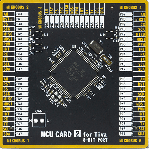
Type
8th Generation
Architecture
ARM Cortex-M4
MCU Memory (KB)
256
Silicon Vendor
Texas Instruments
Pin count
100
RAM (Bytes)
32768
Used MCU Pins
mikroBUS™ mapper
Take a closer look
Click board™ Schematic
Step by step
Project assembly

Start by selecting your development board and Click board™. Begin with the Fusion for ARM v8 as your development board.


Track your results in real time
Application Output
1. Application Output - In Debug mode, the 'Application Output' window enables real-time data monitoring, offering direct insight into execution results. Ensure proper data display by configuring the environment correctly using the provided tutorial.

2. UART Terminal - Use the UART Terminal to monitor data transmission via a USB to UART converter, allowing direct communication between the Click board™ and your development system. Configure the baud rate and other serial settings according to your project's requirements to ensure proper functionality. For step-by-step setup instructions, refer to the provided tutorial.

3. Plot Output - The Plot feature offers a powerful way to visualize real-time sensor data, enabling trend analysis, debugging, and comparison of multiple data points. To set it up correctly, follow the provided tutorial, which includes a step-by-step example of using the Plot feature to display Click board™ readings. To use the Plot feature in your code, use the function: plot(*insert_graph_name*, variable_name);. This is a general format, and it is up to the user to replace 'insert_graph_name' with the actual graph name and 'variable_name' with the parameter to be displayed.

Software Support
Library Description
This library contains API for Boost Click driver.
Key functions:
boost_write_byte- Generic write 14-bit data functionboost_read_byte- Generic read 22-bit of data functionboost_set_configuration- Set configuration function
Open Source
Code example
The complete application code and a ready-to-use project are available through the NECTO Studio Package Manager for direct installation in the NECTO Studio. The application code can also be found on the MIKROE GitHub account.
/*!
 * \file
 * \brief Boost Click example
 *
 * # Description
 * Boost Click provides an adjustable output voltage through the onboard DAC that drives the FB
 * pin of the MIC2606 to set desired output voltage.
 *
 * The demo application is composed of two sections :
 *
 * ## Application Init
 * Initializes SPI driver for serial communication and puts the device to power ON state.
 * Also, initializes logger module for message and results sending.
 *
 * ## Application Task
 * This is a example which demonstrates the use of Boost Click board.
 * Boost Click communicates with register via SPI by reading from MCP3551 chip and writing DAC value to the MCP4921 chip.
 * This example periodicaly increases and decreases voltage in range between 15 and 30 Volts.
 * All data logs write on usb uart for aproximetly every 1 sec.
 *
 *
 * \author Nemanja Medakovic
 *
 */
// ------------------------------------------------------------------- INCLUDES

#include "board.h"
#include "log.h"
#include "boost.h"

// ------------------------------------------------------------------ VARIABLES

static boost_t boost;
static log_t logger;

// ------------------------------------------------------ APPLICATION FUNCTIONS

void application_init ( void )
{
    log_cfg_t log_cfg;

    /**
     * Logger initialization.
     * Default baud rate: 115200
     * Default log level: LOG_LEVEL_DEBUG
     * @note If USB_UART_RX and USB_UART_TX
     * are defined as HAL_PIN_NC, you will
     * need to define them manually for log to work.
     * See @b LOG_MAP_USB_UART macro definition for detailed explanation.
     */
    LOG_MAP_USB_UART( log_cfg );
    log_init( &logger, &log_cfg );
    log_info( &logger, "---- Application Init... ----" );

    boost_cfg_t boost_cfg;

    //  Click initialization.

    boost_cfg_setup( &boost_cfg );
    BOOST_MAP_MIKROBUS( boost_cfg, MIKROBUS_1 );

    if ( boost_init( &boost, &boost_cfg ) == BOOST_ERROR )
    {
        log_info( &logger, "---- Application Init Error. ----" );
        log_info( &logger, "---- Please, run program again... ----" );

        for ( ; ; );
    }

    log_info( &logger, "---- Application Init Done. ----" );

    boost_device_enable( &boost );

    log_info( &logger, "---- Application Running... ----\n" );
}

void application_task ( void )
{
    for ( uint16_t dac_value = 0; ; dac_value += 100 )
    {
        if ( boost_dac_write( &boost, dac_value ) == BOOST_ERROR )
        {
            break;
        }

        log_printf( &logger, " DAC value [12-bit] : %u\r\n", dac_value );
        Delay_ms ( 1000 );

        log_printf( &logger, " VOUT value [V] : %.3f\r\n\n", boost_vout_read( &boost ) );
        Delay_ms ( 1000 );
    }
}

int main ( void )
{
    /* Do not remove this line or clock might not be set correctly. */
    #ifdef PREINIT_SUPPORTED
    preinit();
    #endif

    application_init( );

    for ( ; ; )
    {
        application_task( );
    }

    return 0;
}


// ------------------------------------------------------------------------ END
Additional Support
Resources
Category:Boost