Upgrade your supply needs with TPS61391 and PIC18F57Q43
Unleash the Boost!

Published May 27, 2023
Click board™
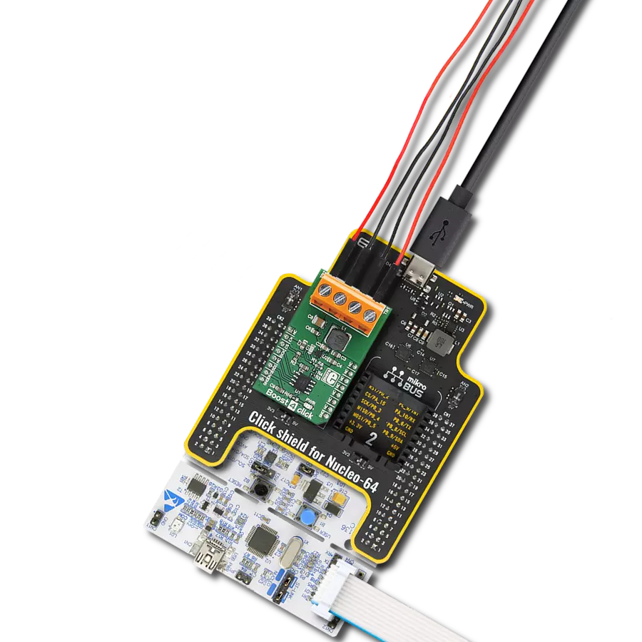
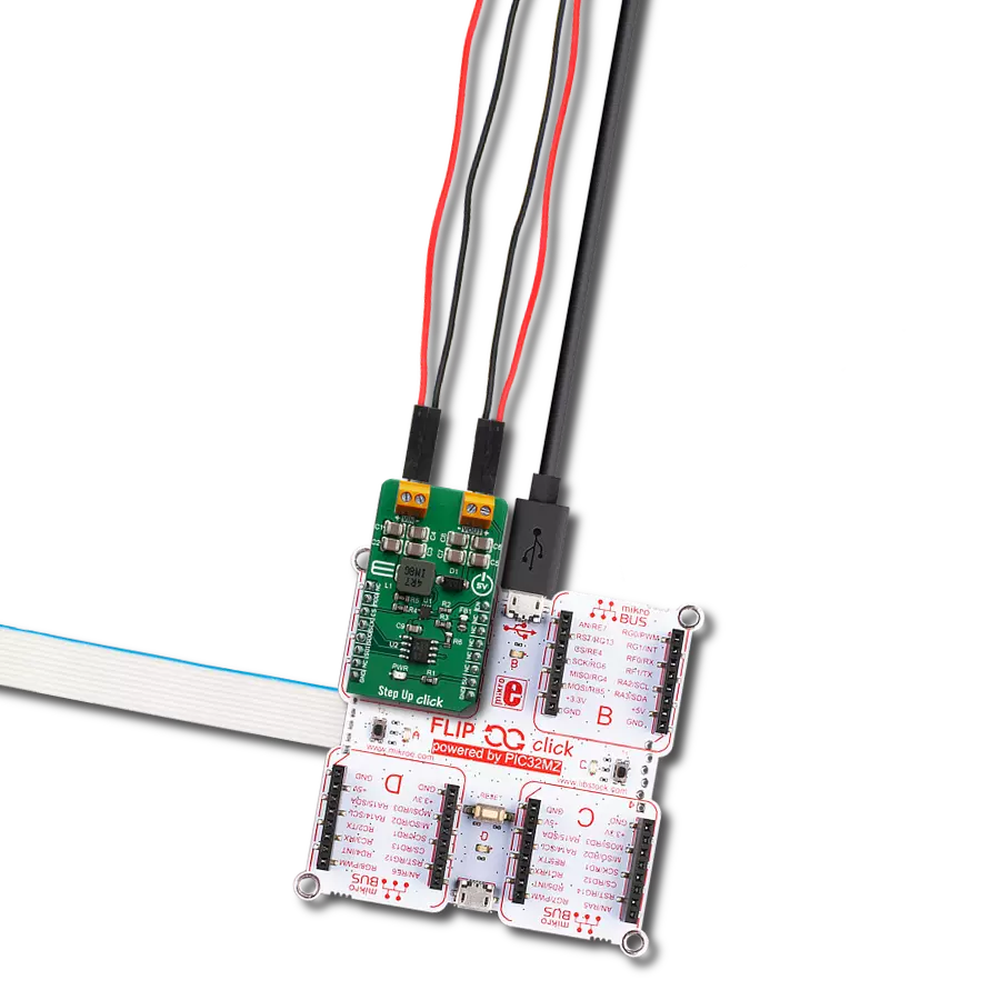
Boost 3 Click
Dev. board
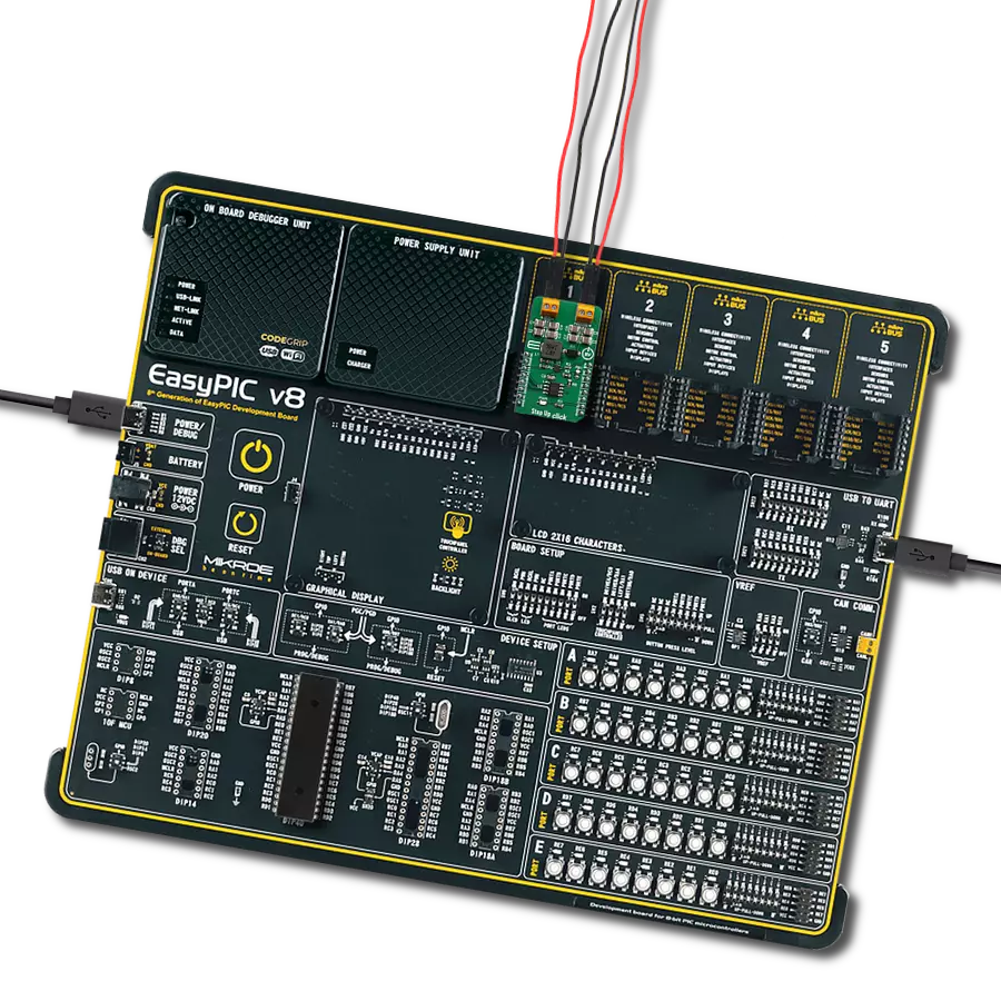
Fusion for PIC v8
Compiler
NECTO Studio
MCU
PIC18F57Q43
Add a boost converter to your solution today and enjoy seamless power management
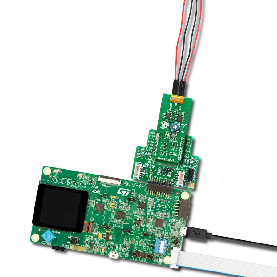
A
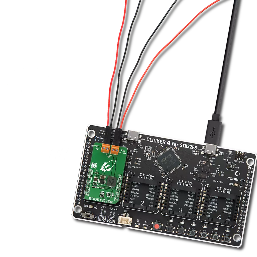
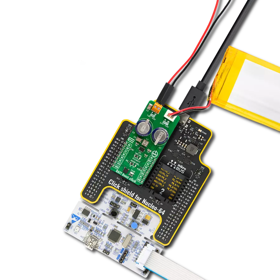
A
Hardware Overview
How does it work?
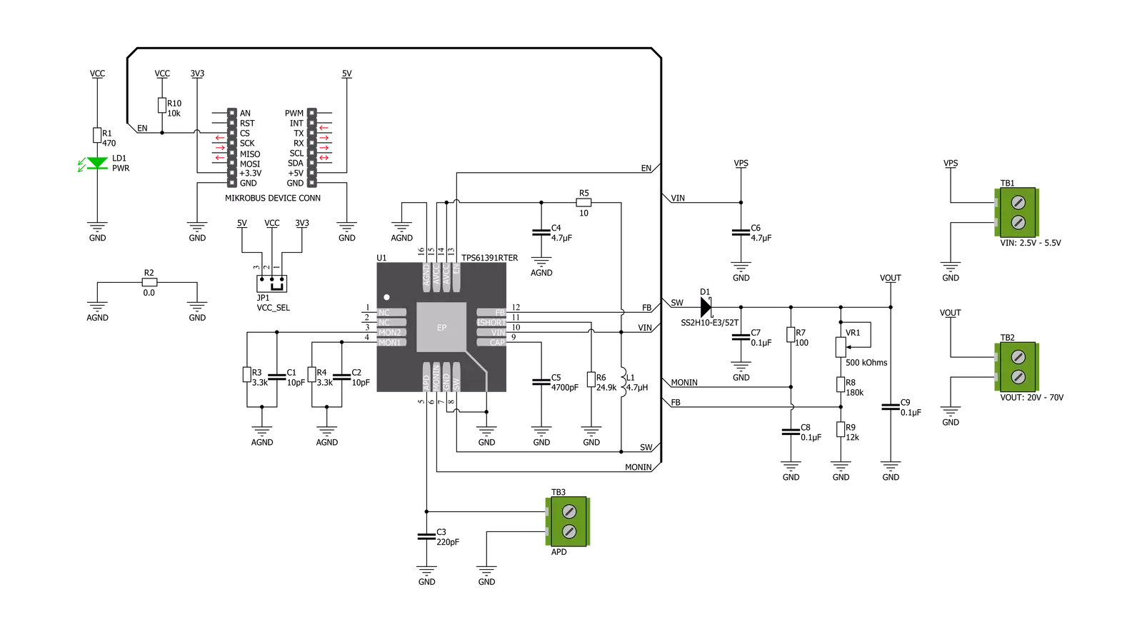
Boost 3 Click is based on the TPS61391, a 700-kHz pulse-width modulating (PWM) Step-Up converter with a 70V switch FET from Texas Instruments. It supports an input voltage of up to 5.5V and operates at a 700 kHz pulse-width modulation (PWM), crossing the whole load range. There are two ratio options for the current proportional to the APD current: MON1 (4:5) and MON2 (1:5). By connecting an additional RC filter for low ripple applications from the mirror output pins to the GND, the current flowing through the APD is converted into the voltage crossing the resistor from MON1/MON2 pins to GND. Additionally, high-power optical protection, with a response time typically of 0.5 μs, is integrated by clamping the pre-set current limit (programmed by the R6 resistor) and could recover automatically when the high optical power is removed. The output voltage of the TPS61391 is externally adjustable using a resistor divider network. The equation gives the relationship between the output voltage and the resistor divider: VOUT = ( VREF + 0.1V ) * ( 1 + ( VR1 + R8 ) / R9 ) [V], where VREF has a typical
value of 1.2V.When the potentiometer has a 0V value, the output voltage has its minimum value of 20V. Increasing the resistance of a potentiometer and reaching its maximum value of 500kΩ, the output voltage reaches its maximum value of 70V. The potentiometer featured on the Boost 3 Click can change the feedback, thus influencing a change in the output voltage. This feature makes the Click board™ extremely practical because you can get a wide voltage range with a simple potentiometer turn. Boost 3 Click communicates with MCU using only one GPIO pin routed on the CS pin of the mikroBUS™ socket labeled as EN. An under-voltage lockout (UVLO) circuit stops the operation of the converter when the input voltage drops below the typical UVLO threshold of 2.5 V. When the input voltage is above the maximal UVLO rising threshold of 2.5 V, and the EN pin is pulled above the high threshold (1.2V minimum), the TPS61391 is enabled. When the EN pin is pulled below the low threshold (0.4 maximum), the device goes into Shutdown Mode.
It also possesses the output terminal labeled APD used for biasing and monitoring the avalanche photodiodes (APD) and high optical power protection. This line has an additional FET in a series of power-path connecting with the APD output terminal. When the current flowing through the external APD exceeds the short protection threshold, set by connecting the resistor from R6 to the ground, the on-resistance of the internal FET becomes larger to clamp the current within the protection threshold by lowering the APD bias voltage. It typically takes 0.5μs for the FET to respond in case of high optical power occurring. When the high optical power condition is released, the TPS61391 recovers automatically back to Normal Operation Mode. This Click board™ can operate with either 3.3V or 5V logic voltage levels selected via the VCC SEL jumper. This way, both 3.3V and 5V capable MCUs can use the communication lines properly. However, the Click board™ comes equipped with a library containing easy-to-use functions and an example code that can be used, as a reference, for further development.

Features overview
Development board
Fusion for PIC v8 is a development board specially designed for the needs of rapid development of embedded applications. It supports a wide range of microcontrollers, such as different PIC, dsPIC, PIC24, and PIC32 MCUs regardless of their number of pins, and a broad set of unique functions, such as the first-ever embedded debugger/programmer over WiFi. The development board is well organized and designed so that the end-user has all the necessary elements, such as switches, buttons, indicators, connectors, and others, in one place. Thanks to innovative manufacturing technology, Fusion for PIC v8 provides a fluid and immersive working experience, allowing access anywhere and under any
circumstances at any time. Each part of the Fusion for PIC v8 development board contains the components necessary for the most efficient operation of the same board. In addition to the advanced integrated CODEGRIP programmer/debugger module, which offers many valuable programming/debugging options and seamless integration with the Mikroe software environment, the board also includes a clean and regulated power supply module for the development board. It can use a wide range of external power sources, including a battery, an external 12V power supply, and a power source via the USB Type-C (USB-C) connector. Communication options such as USB-UART, USB
HOST/DEVICE, CAN (on the MCU card, if supported), and Ethernet are also included, including the well-established mikroBUS™ standard, a standardized socket for the MCU card (SiBRAIN standard), and two display options (graphical and character-based LCD). Fusion for PIC v8 is an integral part of the Mikroe ecosystem for rapid development. Natively supported by Mikroe software tools, it covers many aspects of prototyping and development thanks to a considerable number of different Click boards™ (over a thousand boards), the number of which is growing every day.

Microcontroller Overview
MCU Card / MCU
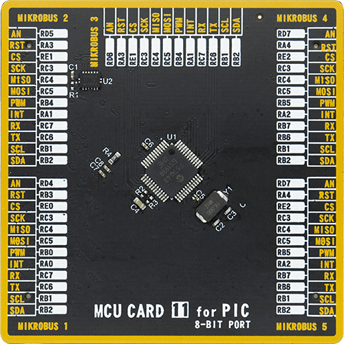
Type
8th Generation
Architecture
PIC
MCU Memory (KB)
128
Silicon Vendor
Microchip
Pin count
48
RAM (Bytes)
8196
Used MCU Pins
mikroBUS™ mapper
Take a closer look
Click board™ Schematic
Step by step
Project assembly

Start by selecting your development board and Click board™. Begin with the Fusion for PIC v8 as your development board.


Track your results in real time
Application Output
1. Application Output - In Debug mode, the 'Application Output' window enables real-time data monitoring, offering direct insight into execution results. Ensure proper data display by configuring the environment correctly using the provided tutorial.

2. UART Terminal - Use the UART Terminal to monitor data transmission via a USB to UART converter, allowing direct communication between the Click board™ and your development system. Configure the baud rate and other serial settings according to your project's requirements to ensure proper functionality. For step-by-step setup instructions, refer to the provided tutorial.

3. Plot Output - The Plot feature offers a powerful way to visualize real-time sensor data, enabling trend analysis, debugging, and comparison of multiple data points. To set it up correctly, follow the provided tutorial, which includes a step-by-step example of using the Plot feature to display Click board™ readings. To use the Plot feature in your code, use the function: plot(*insert_graph_name*, variable_name);. This is a general format, and it is up to the user to replace 'insert_graph_name' with the actual graph name and 'variable_name' with the parameter to be displayed.

Software Support
Library Description
This library contains API for Boost 3 Click driver.
Key functions:
void boost3_dev_enable ( uint8_t state );- Function is used to enable or disable the device.
Open Source
Code example
The complete application code and a ready-to-use project are available through the NECTO Studio Package Manager for direct installation in the NECTO Studio. The application code can also be found on the MIKROE GitHub account.
/*!
 * \file
 * \brief Boost 3 Click example
 *
 * # Description
 * Boost 3 Click provides an adjustable output voltage through the onboard
 * potentiometer. The chip is a 700-kHz pulse-width modulating (PWM) step-up
 * converter with an 85-V switch FET with an input ranging from 2.5 V to 5.5 V.
 *
 * The demo application is composed of two sections :
 *
 * ## Application Init
 * Initializes GPIO and LOG structures, and set CS pin as output.
 *
 * ## Application Task
 * Turns ON the device for 10 seconds and then turns it OFF for 3 seconds.
 * It also displays appropriate messages on the USB UART.
 *
 * \author MikroE Team
 *
 */
// ------------------------------------------------------------------- INCLUDES

#include "board.h"
#include "log.h"
#include "boost3.h"

// ------------------------------------------------------------------ VARIABLES

static boost3_t boost3;
static log_t logger;

// ------------------------------------------------------ APPLICATION FUNCTIONS

void application_init ( void )
{
    log_cfg_t log_cfg;
    boost3_cfg_t cfg;

    /**
     * Logger initialization.
     * Default baud rate: 115200
     * Default log level: LOG_LEVEL_DEBUG
     * @note If USB_UART_RX and USB_UART_TX
     * are defined as HAL_PIN_NC, you will
     * need to define them manually for log to work.
     * See @b LOG_MAP_USB_UART macro definition for detailed explanation.
     */
    LOG_MAP_USB_UART( log_cfg );
    log_init( &logger, &log_cfg );
    log_info( &logger, "---- Application Init ----" );

    //  Click initialization.

    boost3_cfg_setup( &cfg );
    BOOST3_MAP_MIKROBUS( cfg, MIKROBUS_1 );
    boost3_init( &boost3, &cfg );
}

void application_task ( void )
{
    boost3_dev_enable( &boost3, BOOST3_ENABLE );

    log_printf( &logger, "The Click board is enabled!\r\n" );
    log_printf( &logger, "Please use the on-board potentiometer" );
    log_printf( &logger, " to adjust the voltage output.\r\n" );
    log_printf( &logger, "--------------------------------\r\n" );
    // 10 seconds delay
    Delay_ms ( 1000 );
    Delay_ms ( 1000 );
    Delay_ms ( 1000 );
    Delay_ms ( 1000 );
    Delay_ms ( 1000 );
    Delay_ms ( 1000 );
    Delay_ms ( 1000 );
    Delay_ms ( 1000 );
    Delay_ms ( 1000 );
    Delay_ms ( 1000 );

    boost3_dev_enable( &boost3, BOOST3_DISABLE );
    log_printf( &logger, "The Click board is turned OFF!\r\n" );
    log_printf( &logger, "--------------------------------\r\n" );
    Delay_ms ( 1000 );
    Delay_ms ( 1000 );
    Delay_ms ( 1000 );
}

int main ( void )
{
    /* Do not remove this line or clock might not be set correctly. */
    #ifdef PREINIT_SUPPORTED
    preinit();
    #endif

    application_init( );

    for ( ; ; )
    {
        application_task( );
    }

    return 0;
}


// ------------------------------------------------------------------------ END