Save calibration data and system logs with M95P32-I and PIC18F45K40
Infinite ideas, instant recall

Published Aug 24, 2023
Click board™
EEPROM 9 Click
Dev Board
EasyPIC v7a
Compiler
NECTO Studio
MCU
PIC18F45K40
Our EEPROM solution guarantees secure data storage, which is ideal for sensitive information such as encryption keys, boot sequences, and critical system parameters
A
A
Hardware Overview
How does it work?
EEPROM 9 Click is based on the M95P32-I, a 32Mbit SPI page EEPROM device from STMicroelectronics, divided into 8192 erasable pages of 512 bytes (organized either as 1024 erasable sectors of 4 Kbytes, 64 erasable blocks of 64 Kbytes or as an entirely erasable array). The M95P32-I is manufactured with ST's advanced proprietary NVM technology and offers byte flexibility, page alterability, high page cycling performance, and ultra-low power consumption. It is highly reliable, lasting 500k write cycles with 100 years of data retention (10 years after 500k cycles), which makes it suitable for various applications where dependable nonvolatile memory storage is essential. This Click board™ communicates with MCU using the SPI serial interface that supports the two most common modes, SPI Mode 0 and 3, with a maximum SPI frequency of 80MHz.
As mentioned, the M95P32-I offers byte and page write instructions of up to 512 bytes. Write instructions consist of self-timed auto-erase and program operations, resulting in flexible data byte management. It also accepts page/block/sector/chip erase commands to set the memory to an erased state. The memory can then be fast-programmed by pages of 512 bytes and further optimized using the "page program with buffer load" to hide the SPI communication latency. Additional status, configuration, and volatile registers set the desired device configuration, while the safety register gives device status information. In addition to the SPI communication, the EEPROM 9 Click has two additional pins used for Write Protection and Communication Hold function routed to the WP and HLD pins of the mikroBUS™ socket.
The HLD pin of the mikroBUS™ socket can be used to pause the serial communication with the M95P32-I without deselecting the device. The configurable Write Protection function routed to the WP pin of the mikroBUS™ socket allows the user to freeze the memory area protected against Write instructions in a read-only mode (as specified by the values in the BPx and TB bits of the STATUS register). This Click board™ can be operated only with a 3.3V logic voltage level. The board must perform appropriate logic voltage level conversion before using MCUs with different logic levels. Also, it comes equipped with a library containing functions and an example code that can be used, as a reference, for further development.


Features overview
Development board
EasyPIC v7a is the seventh generation of PIC development boards specially designed for the needs of rapid development of embedded applications. It supports a wide range of 8-bit PIC microcontrollers from Microchip and has a broad set of unique functions, such as the first-ever embedded debugger/programmer over USB-C. The development board is well organized and designed so that the end-user has all the necessary elements in one place, such as switches, buttons, indicators, connectors, and others. With four different connectors for each port, EasyPIC v7a allows you to connect accessory boards, sensors, and custom electronics more efficiently than ever. Each part of the EasyPIC v7a development board
contains the components necessary for the most efficient operation of the same board. In addition to the advanced integrated CODEGRIP programmer/debugger module, which offers many valuable programming/debugging options and seamless integration with the Mikroe software environment, the board also includes a clean and regulated power supply module for the development board. It can use various external power sources, including an external 12V power supply, 7-23V AC or 9-32V DC via DC connector/screw terminals, and a power source via the USB Type-C (USB-C) connector. Communication options such as USB-UART and RS-232 are also included, alongside the well-
established mikroBUS™ standard, three display options (7-segment, graphical, and character-based LCD), and several different DIP sockets. These sockets cover a wide range of 8-bit PIC MCUs, from PIC10F, PIC12F, PIC16F, PIC16Enh, PIC18F, PIC18FJ, and PIC18FK families. EasyPIC v7a is an integral part of the Mikroe ecosystem for rapid development. Natively supported by Mikroe software tools, it covers many aspects of prototyping and development thanks to a considerable number of different Click boards™ (over a thousand boards), the number of which is growing every day.

Microcontroller Overview
MCU Card / MCU
Architecture
PIC
MCU Memory (KB)
32
Silicon Vendor
Microchip
Pin count
40
RAM (Bytes)
2048
Used MCU Pins
mikroBUS™ mapper
Take a closer look
Schematic

Step by step
Project assembly

Start by selecting your development board and Click board™. Begin with the EasyPIC v7a as your development board.


Track your results in real time
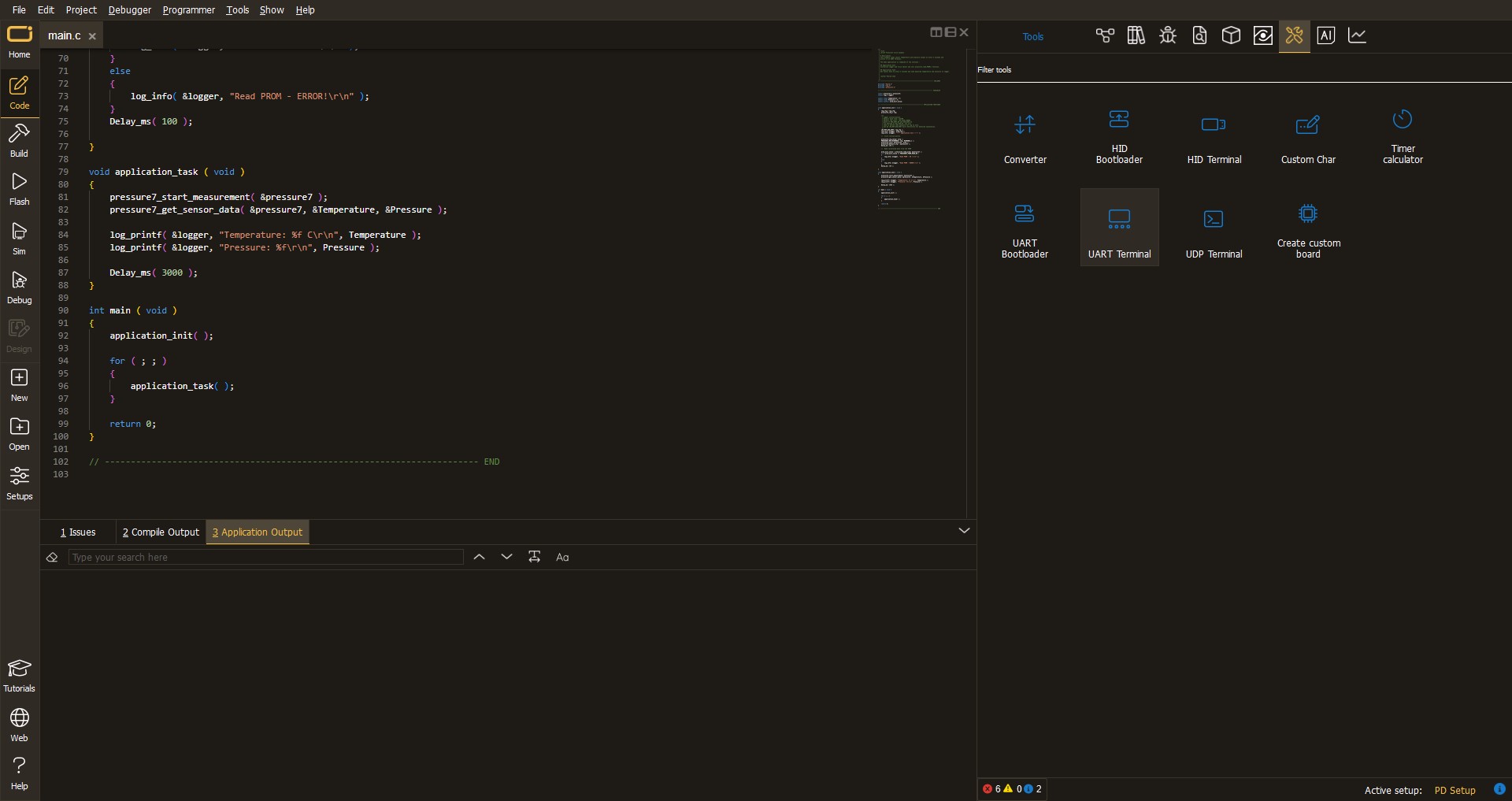
Application Output
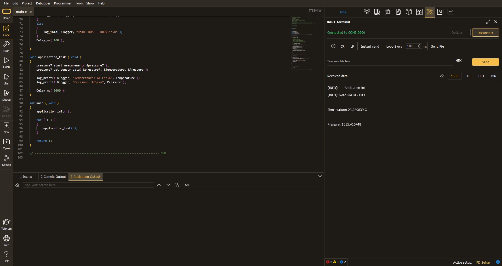
After pressing the "FLASH" button on the left-side panel, it is necessary to open the UART terminal to display the achieved results. By clicking on the Tools icon in the right-hand panel, multiple different functions are displayed, among which is the UART Terminal. Click on the offered "UART Terminal" icon.
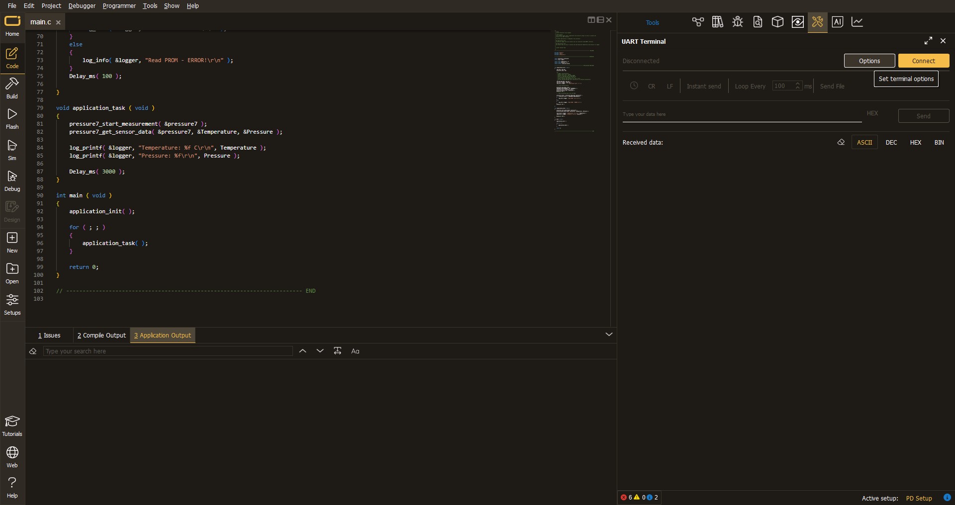
Once the UART terminal is opened, the window takes on a new form. At the top of the tab are two buttons, one for adjusting the parameters of the UART terminal and the other for connecting the UART terminal. The tab's lower part is reserved for displaying the achieved results. Before connecting, the terminal has a Disconnected status, indicating that the terminal is not yet active. Before connecting, it is necessary to check the set parameters of the UART terminal. Click on the "OPTIONS" button.
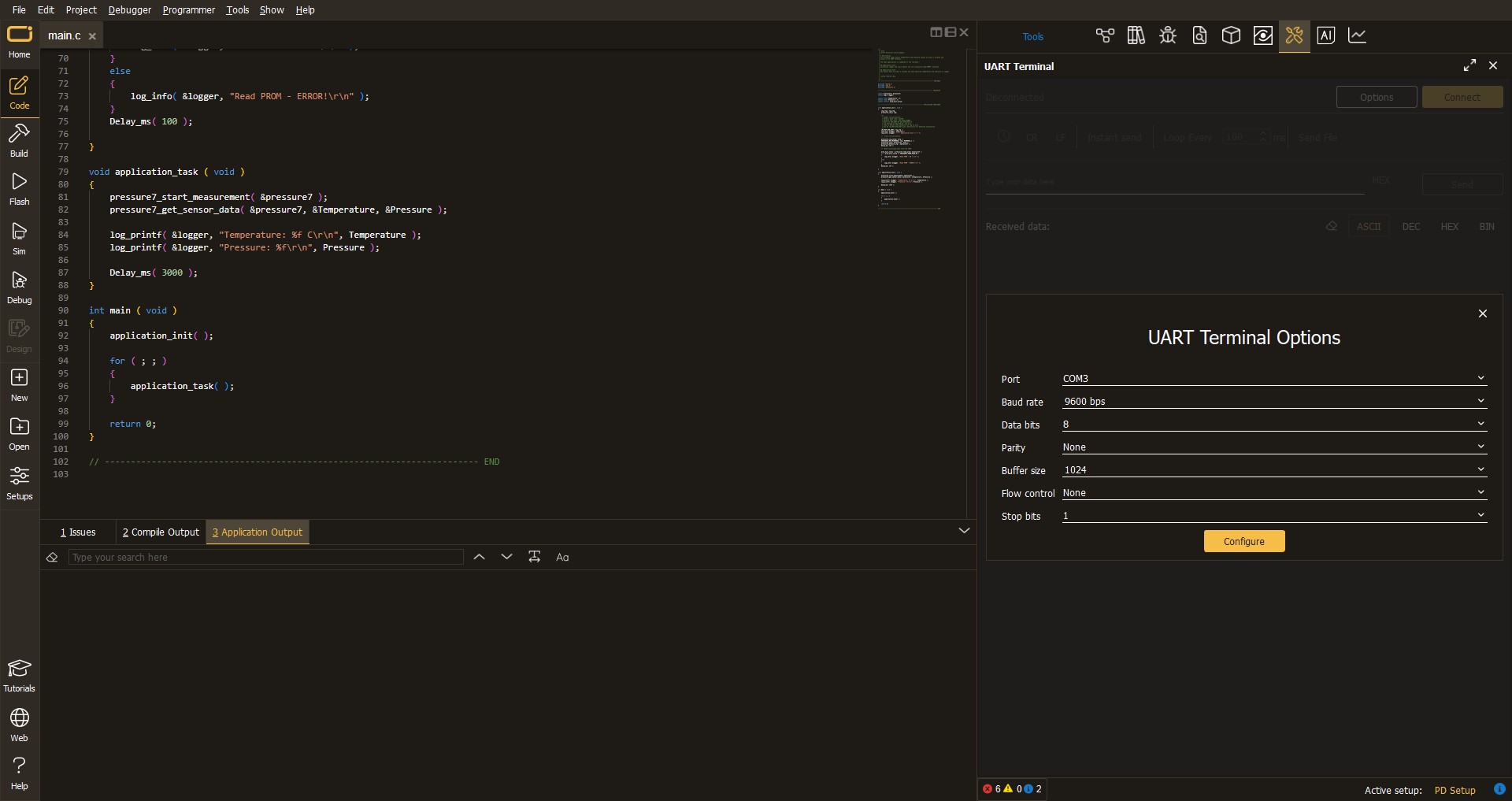
In the newly opened UART Terminal Options field, we check if the terminal settings are correct, such as the set port and the Baud rate of UART communication. If the data is not displayed properly, it is possible that the Baud rate value is not set correctly and needs to be adjusted to 115200. If all the parameters are set correctly, click on "CONFIGURE".
The next step is to click on the "CONNECT" button, after which the terminal status changes from Disconnected to Connected in green, and the data is displayed in the Received data field.
Software Support
Library Description
This library contains API for EEPROM 9 Click driver.
Key functions:
eeprom9_set_write_enable- EEPROM 9 enable write functioneeprom9_read_memory- EEPROM 9 memory reading functioneeprom9_block_erase- EEPROM 9 memory block erase function.
Open Source
Code example
This example can be found in NECTO Studio. Feel free to download the code, or you can copy the code below.
/*!
 * @file main.c
 * @brief EEPROM 9 Click example
 *
 * # Description
 * This is an example that demonstrates the use of the EEPROM 9 Click board.
 *
 * The demo application is composed of two sections :
 *
 * ## Application Init
 * Initializes the driver and USB UART logging, disables hold and write protection.
 *
 * ## Application Task
 * Writes a desired number of data bytes to the EEPROM 9 memory into a specified address,
 * and verifies that it is written correctly by reading from the same memory location.
 *
 * @author Stefan Ilic
 *
 */

#include "board.h"
#include "log.h"
#include "eeprom9.h"

static eeprom9_t eeprom9;
static log_t logger;
static char demo_data[ 9 ] = { 'M', 'i', 'k', 'r', 'o', 'E', 13 ,10 , 0 };

#define MEMORY_ADDRESS  0x0300

void application_init ( void )
{
    log_cfg_t log_cfg;  /**< Logger config object. */
    eeprom9_cfg_t eeprom9_cfg;  /**< Click config object. */
    id_data_t id_data;

    /**
     * Logger initialization.
     * Default baud rate: 115200
     * Default log level: LOG_LEVEL_DEBUG
     * @note If USB_UART_RX and USB_UART_TX
     * are defined as HAL_PIN_NC, you will
     * need to define them manually for log to work.
     * See @b LOG_MAP_USB_UART macro definition for detailed explanation.
     */
    LOG_MAP_USB_UART( log_cfg );
    log_init( &logger, &log_cfg );
    log_info( &logger, " Application Init " );

    // Click initialization.
    eeprom9_cfg_setup( &eeprom9_cfg );
    EEPROM9_MAP_MIKROBUS( eeprom9_cfg, MIKROBUS_1 );
    if ( SPI_MASTER_ERROR == eeprom9_init( &eeprom9, &eeprom9_cfg ) )
    {
        log_error( &logger, " Communication init." );
        for ( ; ; );
    }

    eeprom9_read_identification( &eeprom9, &id_data );
    if ( EEPROM9_ST_MANUFACTURER_CODE != id_data.manufact_code )
    {
        log_error( &logger, " Communication error." );
        for ( ; ; );
    }
    log_printf( &logger, " Manufacturer code: 0x%.2X \r\n", ( uint16_t ) id_data.manufact_code );

    log_printf( &logger, " Disabling Hold \r\n" );
    eeprom9_set_hold( &eeprom9, EEPROM9_HOLD_DISABLE );
    Delay_ms( 100 );

    log_printf( &logger, " Disabling Write Protection \r\n" );
    eeprom9_set_write_protection( &eeprom9, EEPROM9_WRITE_PROTECT_DISABLE );
    Delay_ms( 100 );

    log_info( &logger, " Application Task " );
    log_printf( &logger, " - - - - - - - - - - - \r\n" );
}

void application_task ( void )
{
    char rx_data[ 9 ] = { 0 };

    eeprom9_set_write_enable( &eeprom9, EEPROM9_WRITE_ENABLE );
    Delay_ms( 10 );

    eeprom9_write_memory( &eeprom9, MEMORY_ADDRESS, demo_data, 9 );
    log_printf( &logger, " Write data: %s", demo_data );
    Delay_ms( 100 );

    eeprom9_read_memory( &eeprom9, MEMORY_ADDRESS, rx_data, 9 );
    log_printf( &logger, " Read data: %s", rx_data );
    log_printf( &logger, " - - - - - - - - - - - \r\n" );

    Delay_ms( 1000 );

}

void main ( void )
{
    application_init( );

    for ( ; ; )
    {
        application_task( );
    }
}

// ------------------------------------------------------------------------ END


