Swiftly recover from unexpected errors with AT21CS01 and PIC18F57Q43
Single-wire serial EEPROM

Published Feb 13, 2024
Click board™
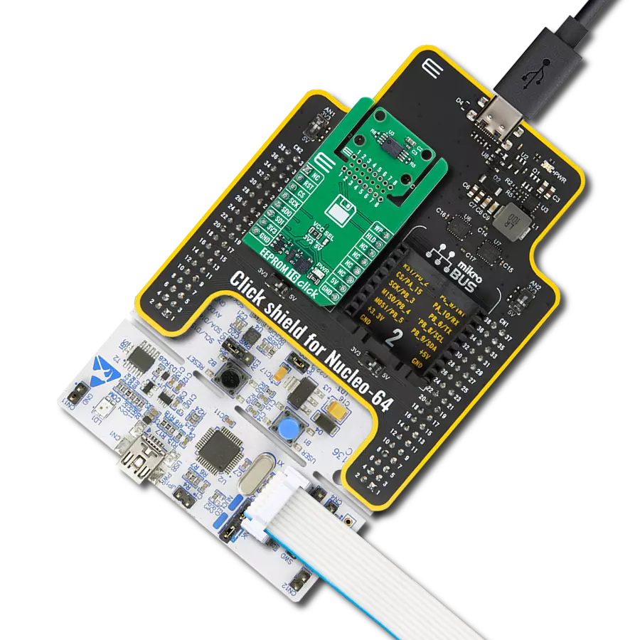
SWI EEPROM Click
Dev. board
Curiosity Nano with PIC18F57Q43
Compiler
NECTO Studio
MCU
PIC18F57Q43
Our solution leverages single-wire EEPROM to store calibration values, usage history, and device-specific information, streamlining maintenance and enhancing overall efficiency
A
A
Hardware Overview
How does it work?
SWI EEPROM Click is based on the AT21CS01, 2-pin serial electrically erasable and programmable read-only memory (EEPROM) that harvests energy from the SI/O pin to power the integrated circuit from Microchip Technology. It provides 1,024 bits organized as 128 words of 8 bits each, a security register with a 64-bit factory-programmed serial number, and an extra 16 bytes of user-programmable and permanently lockable storage. It delivers a guaranteed unique serial number for inventory tracking and asset tagging and can always protect the data if needed. The AT21CS01 benefits from 100 years of data retention, combining its unprecedented data storage with excellent energy efficiency. It is characterized
by high reliability and ultra-high writing endurance capability, allowing more than one million cycles for each memory location to meet today's high-write endurance applications' requirements. SWI EEPROM Click communicates with MCU using the Single-Wire interface that, by definition, requires only one data line (and ground) for communication with MCU. The SI/O pin routed to the PWM pin of the mikroBUS™ socket is a bidirectional input/output pin used to serially transfer data to and from the device featuring a maximum 15.4Kbps bit rate in Standard-Speed mode and 125Kbps in High-Speed mode. The AT21CS01 uses a modified I2C interface to extract power from the reading and writing sequences.
The software sequence sent to the device emulates what would be sent to an I2C serial EEPROM, except that a 4-bit opcode replaces a typical 4-bit device type identifier of 1010b in the device address. The device has been architected for rapid deployment and significant reuse of existing I2C firmware. This Click board™ can be operated only with a 3.3V logic voltage level. The board must perform appropriate logic voltage level conversion before using MCUs with different logic levels. Also, it comes equipped with a library containing functions and an example code that can be used, as a reference, for further development.


Features overview
Development board
PIC18F57Q43 Curiosity Nano evaluation kit is a cutting-edge hardware platform designed to evaluate microcontrollers within the PIC18-Q43 family. Central to its design is the inclusion of the powerful PIC18F57Q43 microcontroller (MCU), offering advanced functionalities and robust performance. Key features of this evaluation kit include a yellow user LED and a responsive
mechanical user switch, providing seamless interaction and testing. The provision for a 32.768kHz crystal footprint ensures precision timing capabilities. With an onboard debugger boasting a green power and status LED, programming and debugging become intuitive and efficient. Further enhancing its utility is the Virtual serial port (CDC) and a debug GPIO channel (DGI
GPIO), offering extensive connectivity options. Powered via USB, this kit boasts an adjustable target voltage feature facilitated by the MIC5353 LDO regulator, ensuring stable operation with an output voltage ranging from 1.8V to 5.1V, with a maximum output current of 500mA, subject to ambient temperature and voltage constraints.

Microcontroller Overview
MCU Card / MCU

Architecture
PIC
MCU Memory (KB)
128
Silicon Vendor
Microchip
Pin count
48
RAM (Bytes)
8196
You complete me!
Accessories
Curiosity Nano Base for Click boards is a versatile hardware extension platform created to streamline the integration between Curiosity Nano kits and extension boards, tailored explicitly for the mikroBUS™-standardized Click boards and Xplained Pro extension boards. This innovative base board (shield) offers seamless connectivity and expansion possibilities, simplifying experimentation and development. Key features include USB power compatibility from the Curiosity Nano kit, alongside an alternative external power input option for enhanced flexibility. The onboard Li-Ion/LiPo charger and management circuit ensure smooth operation for battery-powered applications, simplifying usage and management. Moreover, the base incorporates a fixed 3.3V PSU dedicated to target and mikroBUS™ power rails, alongside a fixed 5.0V boost converter catering to 5V power rails of mikroBUS™ sockets, providing stable power delivery for various connected devices.

Used MCU Pins
mikroBUS™ mapper
Take a closer look
Click board™ Schematic

Step by step
Project assembly

Start by selecting your development board and Click board™. Begin with the Curiosity Nano with PIC18F57Q43 as your development board.


Software Support
Library Description
This library contains API for SWI EEPROM Click driver.
Key functions:
swieeprom_mem_write_page- This function writes data to the specified memory address pageswieeprom_mem_read- This function reads data from the specified memory addressswieeprom_mem_clear- This function clears the whole memory to zero
Open Source
Code example
The complete application code and a ready-to-use project are available through the NECTO Studio Package Manager for direct installation in the NECTO Studio. The application code can also be found on the MIKROE GitHub account.
/*!
 * @file main.c
 * @brief SWI EEPROM Click Example.
 *
 * # Description
 * This example demonstrates the use of SWI EEPROM Click board by writing specified data to
 * the memory and reading it back.
 *
 * The demo application is composed of two sections :
 *
 * ## Application Init
 * Initializes the driver and logger and checks the communication.
 *
 * ## Application Task
 * Writes the specified text message to the memory and reads it back. After that, erases
 * the whole memory and tries to read the same message verifying that the memory is erased.
 * All data is being displayed on the USB UART where you can track the program flow.
 *
 * @note
 * This application is written for the following MCUs and specifically for MIKROBUS 1:
 * STM32F407ZG, MK64FN1M0VDC12, TM4C129XNCZAD, GD32VF103VBT6, PIC32MX795F512L
 * In order to use it on another MCUs the pin_x functions must be defined in a way
 * it matches the required timing specifications for the Single Wire interface.
 *
 * @author Stefan Filipovic
 *
 */

#include "board.h"
#include "log.h"
#include "swieeprom.h"

#define DEMO_TEXT_MESSAGE       "MIKROE"
#define STARTING_ADDRESS        0x00

static swieeprom_t swieeprom;   /**< SWI EEPROM Click driver object. */
static log_t logger;    /**< Logger object. */

/**
 * @brief Pin init function.
 * @details This function initializes the SIO pin.
 * @return None.
 * @note By default it initializes the SIO pin to the PWM pin from MIKROBUS 1.
 * The implementation differs from MCU to MCU.
 */
static void pin_init( void );

/**
 * @brief Pin low function.
 * @details This function sets the SIO pin to LOW logic level.
 * @return None.
 * @note The pin it uses should match the one that is initialized using the pin_init function.
 * The implementation differs from MCU to MCU.
 */
static void pin_low( void );

/**
 * @brief Pin release function.
 * @details This function releases the SIO pin by setting it to digital input.
 * @return None.
 * @note The pin it uses should match the one that is initialized using the pin_init function.
 * The implementation differs from MCU to MCU.
 */
static void pin_release( void );

/**
 * @brief Pin get function.
 * @details This function returns the SIO pin logic state.
 * @return Pin logic state.
 * @note The pin it uses should match the one that is initialized using the pin_init function.
 * The implementation differs from MCU to MCU.
 */
static uint8_t pin_get( void );

/**
 * @brief SWI EEPROM reset function.
 * @details This function initializes the SIO pin and performs the SWI reset.
 * @return @li @c  0 - Success,
 *         @li @c -1 - Error.
 * See #err_t definition for detailed explanation.
 * @note None.
 */
static err_t swieeprom_reset ( void );

/**
 * @brief SWI EEPROM start stop function.
 * @details This function sends the SWI start/stop signal.
 * @return None.
 * @note None.
 */
static void swieeprom_start_stop ( void );

/**
 * @brief SWI EEPROM logic write 0 function.
 * @details This function sends the SWI logic zero signal.
 * @return None.
 * @note None.
 */
static void swieeprom_logic_write_0 ( void );

/**
 * @brief SWI EEPROM logic write 1 function.
 * @details This function sends the SWI logic one signal.
 * @return None.
 * @note None.
 */
static void swieeprom_logic_write_1 ( void );

/**
 * @brief SWI EEPROM logic read function.
 * @details This function reads the SWI logic state.
 * @return Logic state.
 * @note None.
 */
static uint8_t swieeprom_logic_read ( void );

void application_init ( void )
{
    log_cfg_t log_cfg;  /**< Logger config object. */

    /**
     * Logger initialization.
     * Default baud rate: 115200
     * Default log level: LOG_LEVEL_DEBUG
     * @note If USB_UART_RX and USB_UART_TX
     * are defined as HAL_PIN_NC, you will
     * need to define them manually for log to work.
     * See @b LOG_MAP_USB_UART macro definition for detailed explanation.
     */
    LOG_MAP_USB_UART( log_cfg );
    log_init( &logger, &log_cfg );
    log_info( &logger, " Application Init " );

    // Click initialization.
    swieeprom.swi_reset = &swieeprom_reset;
    swieeprom.swi_start_stop = &swieeprom_start_stop;
    swieeprom.swi_logic_0 = &swieeprom_logic_write_0;
    swieeprom.swi_logic_1 = &swieeprom_logic_write_1;
    swieeprom.swi_logic_read = &swieeprom_logic_read;
    if ( SWIEEPROM_ERROR == swieeprom_init ( &swieeprom ) )
    {
        log_error( &logger, " Communication init." );
        for ( ; ; );
    }

    if ( SWIEEPROM_ERROR == swieeprom_check_communication ( &swieeprom ) )
    {
        log_error( &logger, " Check communication." );
        for ( ; ; );
    }

    log_info( &logger, " Application Task " );
}

void application_task ( void )
{
    uint8_t data_buf[ 8 ] = { 0 };
    // Write data to the specified address
    log_printf ( &logger, " Memory address: 0x%.2X\r\n", ( uint16_t ) STARTING_ADDRESS );
    memcpy ( data_buf, DEMO_TEXT_MESSAGE, strlen ( DEMO_TEXT_MESSAGE ) );
    if ( SWIEEPROM_OK == swieeprom_mem_write_page ( &swieeprom, STARTING_ADDRESS,
                                                    data_buf, strlen ( DEMO_TEXT_MESSAGE ) ) )
    {
        log_printf ( &logger, " Write data: %s\r\n", data_buf );
        Delay_ms ( 100 );
    }
    // Read data from the specified address to verify the previous memory write
    memset ( data_buf, 0, sizeof ( data_buf ) );
    if ( SWIEEPROM_OK == swieeprom_mem_read ( &swieeprom, STARTING_ADDRESS,
                                              data_buf, sizeof ( data_buf ) ) )
    {
        log_printf ( &logger, " Read data: %s\r\n", data_buf );
        Delay_ms ( 1000 );
        Delay_ms ( 1000 );
    }
    // Clear whole memory
    if ( SWIEEPROM_OK == swieeprom_mem_clear ( &swieeprom ) )
    {
        log_printf ( &logger, " Memory clear\r\n" );
        Delay_ms ( 100 );
    }
    // Read data from the specified address to verify the previous memory clear
    memset ( data_buf, 0, sizeof ( data_buf ) );
    if ( SWIEEPROM_OK == swieeprom_mem_read ( &swieeprom, STARTING_ADDRESS,
                                              data_buf, sizeof ( data_buf ) ) )
    {
        log_printf ( &logger, " Read data: %s\r\n\n", data_buf );
        Delay_ms ( 1000 );
        Delay_ms ( 1000 );
    }
}

int main ( void )
{
    /* Do not remove this line or clock might not be set correctly. */
    #ifdef PREINIT_SUPPORTED
    preinit();
    #endif

    application_init( );

    for ( ; ; )
    {
        application_task( );
    }

    return 0;
}

#ifdef __MIKROC_AI__
    #ifdef STM32F407ZG
        void pin_init( void )
        {
            digital_in_t sio_in;
            digital_in_init ( &sio_in, PD12 );
        }

        void pin_low( void )
        {
            if ( !GPIOD_MODER.B24 )
            {
                GPIOD_MODER.B24 = 1;
            }
            GPIOD_ODR.B12 = 0;
        }

        void pin_release( void )
        {
            if ( GPIOD_MODER.B24 )
            {
                GPIOD_MODER.B24 = 0;
            }
        }

        uint8_t pin_get( void )
        {
            if ( GPIOD_MODER.B24 )
            {
                GPIOD_MODER.B24 = 0;
            }
            return GPIOD_IDR.B12;
        }
    #elif MK64FN1M0VDC12
        void pin_init( void )
        {
            digital_in_t sio_in;
            digital_in_init ( &sio_in, PE6 );
        }

        void pin_low( void )
        {
            if ( !GPIOE_PDDR.B6 )
            {
                GPIOE_PDDR.B6 = 1;
            }
            GPIOE_PDOR.B6 = 0;
        }

        void pin_release( void )
        {
            if ( GPIOE_PDDR.B6 )
            {
                GPIOE_PDDR.B6 = 0;
            }
        }

        uint8_t pin_get( void )
        {
            if ( GPIOE_PDDR.B6 )
            {
                GPIOE_PDDR.B6 = 0;
            }
            return GPIOE_PDIR.B6;
        }
    #elif TM4C129XNCZAD
        void pin_init( void )
        {
            digital_in_t sio_in;
            digital_in_init ( &sio_in, PD0 );
        }

        void pin_low( void )
        {
            if ( !GPIO_PORTD_AHB_DIR.B0 )
            {
                GPIO_PORTD_AHB_DIR.B0 = 1;
            }
            GPIO_PORTD_AHB_DATA.B0 = 0;
        }

        void pin_release( void )
        {
            if ( GPIO_PORTD_AHB_DIR.B0 )
            {
                GPIO_PORTD_AHB_DIR.B0 = 0;
            }
        }

        uint8_t pin_get( void )
        {
            if ( GPIO_PORTD_AHB_DIR.B0 )
            {
                GPIO_PORTD_AHB_DIR.B0 = 0;
            }
            return GPIO_PORTD_AHB_DATA.B0;
        }
    #elif PIC32MX795F512L
        void pin_init( void )
        {
            digital_in_t sio_in;
            digital_in_init ( &sio_in, PD1 );
        }

        void pin_low( void )
        {
            if ( TRISD1_bit )
            {
                TRISD1_bit = 0;
            }
            LATD1_bit = 0;
        }

        void pin_release( void )
        {
            if ( !TRISD1_bit )
            {
                TRISD1_bit = 1;
            }
        }

        uint8_t pin_get( void )
        {
            if ( !TRISD1_bit )
            {
                TRISD1_bit = 1;
            }
            return RD1_bit;
        }
    #else
        #error "Pin functions are not defined for the selected MCU"
    #endif
#elif __clang__
    #ifdef STM32F407ZG
        #define GPIOD_MODER             ( *( uint32_t * ) 0x40020C00 )
        #define GPIOD_IDR               ( *( uint32_t * ) 0x40020C10 )
        #define GPIOD_ODR               ( *( uint32_t * ) 0x40020C14 )
        #define GPIO_MODER_PIN12_MASK   ( ( uint32_t ) 3 << 24 )
        #define GPIO_MODER_PIN12_INPUT  ( ( uint32_t ) 0 << 24 )
        #define GPIO_MODER_PIN12_OUTPUT ( ( uint32_t ) 1 << 24 )
        #define GPIO_PIN12_MASK         ( ( uint32_t ) 1 << 12 )
        void pin_init( void )
        {
            digital_in_t sio_in;
            digital_in_init ( &sio_in, PD12 );
        }

        void pin_low( void )
        {
            if ( GPIO_MODER_PIN12_OUTPUT != ( GPIOD_MODER & GPIO_MODER_PIN12_MASK ) )
            {
                GPIOD_MODER &= ~GPIO_MODER_PIN12_MASK;
                GPIOD_MODER |= GPIO_MODER_PIN12_OUTPUT;
            }
            GPIOD_ODR &= ~GPIO_PIN12_MASK;
        }

        void pin_release( void )
        {
            if ( GPIO_MODER_PIN12_INPUT != ( GPIOD_MODER & GPIO_MODER_PIN12_MASK ) )
            {
                GPIOD_MODER &= ~GPIO_MODER_PIN12_MASK;
            }
        }

        uint8_t pin_get( void )
        {
            if ( GPIO_MODER_PIN12_INPUT != ( GPIOD_MODER & GPIO_MODER_PIN12_MASK ) )
            {
                GPIOD_MODER &= ~GPIO_MODER_PIN12_MASK;
            }
            return ( GPIO_PIN12_MASK == ( GPIOD_IDR & GPIO_PIN12_MASK ) );
        }
    #elif MK64
        #define GPIOE_PDOR              ( *( uint32_t * ) 0x400FF100 )
        #define GPIOE_PDIR              ( *( uint32_t * ) 0x400FF110 )
        #define GPIOE_PDDR              ( *( uint32_t * ) 0x400FF114 )
        #define GPIO_PDDR_PIN6_INPUT    ( ( uint32_t ) 0 << 6 )
        #define GPIO_PDDR_PIN6_OUTPUT   ( ( uint32_t ) 1 << 6 )
        #define GPIO_PIN6_MASK          ( ( uint32_t ) 1 << 6 )
        void pin_init( void )
        {
            digital_in_t sio_in;
            digital_in_init ( &sio_in, PE6 );
        }

        void pin_low( void )
        {
            if ( GPIO_PDDR_PIN6_OUTPUT != ( GPIOE_PDDR & GPIO_PIN6_MASK ) )
            {
                GPIOE_PDDR |= GPIO_PDDR_PIN6_OUTPUT;
            }
            GPIOE_PDOR &= ~GPIO_PIN6_MASK;
        }

        void pin_release( void )
        {
            if ( GPIO_PDDR_PIN6_INPUT != ( GPIOE_PDDR & GPIO_PIN6_MASK ) )
            {
                GPIOE_PDDR &= ~GPIO_PDDR_PIN6_OUTPUT;
            }
        }

        uint8_t pin_get( void )
        {
            if ( GPIO_PDDR_PIN6_INPUT != ( GPIOE_PDDR & GPIO_PIN6_MASK ) )
            {
                GPIOE_PDDR &= ~GPIO_PDDR_PIN6_OUTPUT;
            }
            return ( GPIO_PIN6_MASK == ( GPIOE_PDIR & GPIO_PIN6_MASK ) );
        }
    #elif TM4C129
        #define GPIOD_PORTD_DIR         ( *( uint32_t * ) 0x4005B400 )
        #define GPIOD_PORTD_DATA        ( *( uint32_t * ) 0x4005B3FC )
        #define GPIO_PORTD_PIN0_INPUT   ( ( uint32_t ) 0 )
        #define GPIO_PORTD_PIN0_OUTPUT  ( ( uint32_t ) 1 )
        #define GPIO_PIN0_MASK          ( ( uint32_t ) 1 )
        void pin_init( void )
        {
            digital_in_t sio_in;
            digital_in_init ( &sio_in, PD0 );
        }

        void pin_low( void )
        {
            if ( GPIO_PORTD_PIN0_OUTPUT != ( GPIOD_PORTD_DIR & GPIO_PIN0_MASK ) )
            {
                GPIOD_PORTD_DIR |= GPIO_PORTD_PIN0_OUTPUT;
            }
            GPIOD_PORTD_DATA &= ~GPIO_PIN0_MASK;
        }

        void pin_release( void )
        {
            if ( GPIO_PORTD_PIN0_INPUT != ( GPIOD_PORTD_DIR & GPIO_PIN0_MASK ) )
            {
                GPIOD_PORTD_DIR &= ~GPIO_PORTD_PIN0_OUTPUT;
            }
        }

        uint8_t pin_get( void )
        {
            if ( GPIO_PORTD_PIN0_INPUT != ( GPIOD_PORTD_DIR & GPIO_PIN0_MASK ) )
            {
                GPIOD_PORTD_DIR &= ~GPIO_PORTD_PIN0_OUTPUT;
            }
            return ( GPIO_PIN0_MASK == ( GPIOD_PORTD_DATA & GPIO_PIN0_MASK ) );
        }
    #else
        #error "Pin functions are not defined for the selected MCU"
    #endif
#elif __GNUC__
    #ifdef STM32F407ZG
        #define GPIOD_MODER             ( *( uint32_t * ) 0x40020C00 )
        #define GPIOD_IDR               ( *( uint32_t * ) 0x40020C10 )
        #define GPIOD_ODR               ( *( uint32_t * ) 0x40020C14 )
        #define GPIO_MODER_PIN12_MASK   ( ( uint32_t ) 3 << 24 )
        #define GPIO_MODER_PIN12_INPUT  ( ( uint32_t ) 0 << 24 )
        #define GPIO_MODER_PIN12_OUTPUT ( ( uint32_t ) 1 << 24 )
        #define GPIO_PIN12_MASK         ( ( uint32_t ) 1 << 12 )
        void pin_init( void )
        {
            digital_in_t sio_in;
            digital_in_init ( &sio_in, PD12 );
        }

        void pin_low( void )
        {
            if ( GPIO_MODER_PIN12_OUTPUT != ( GPIOD_MODER & GPIO_MODER_PIN12_MASK ) )
            {
                GPIOD_MODER &= ~GPIO_MODER_PIN12_MASK;
                GPIOD_MODER |= GPIO_MODER_PIN12_OUTPUT;
            }
            GPIOD_ODR &= ~GPIO_PIN12_MASK;
        }

        void pin_release( void )
        {
            if ( GPIO_MODER_PIN12_INPUT != ( GPIOD_MODER & GPIO_MODER_PIN12_MASK ) )
            {
                GPIOD_MODER &= ~GPIO_MODER_PIN12_MASK;
            }
        }

        uint8_t pin_get( void )
        {
            if ( GPIO_MODER_PIN12_INPUT != ( GPIOD_MODER & GPIO_MODER_PIN12_MASK ) )
            {
                GPIOD_MODER &= ~GPIO_MODER_PIN12_MASK;
            }
            return ( GPIO_PIN12_MASK == ( GPIOD_IDR & GPIO_PIN12_MASK ) );
        }
    #elif MK64
        #define GPIOE_PDOR              ( *( uint32_t * ) 0x400FF100 )
        #define GPIOE_PDIR              ( *( uint32_t * ) 0x400FF110 )
        #define GPIOE_PDDR              ( *( uint32_t * ) 0x400FF114 )
        #define GPIO_PDDR_PIN6_INPUT    ( ( uint32_t ) 0 << 6 )
        #define GPIO_PDDR_PIN6_OUTPUT   ( ( uint32_t ) 1 << 6 )
        #define GPIO_PIN6_MASK          ( ( uint32_t ) 1 << 6 )
        void pin_init( void )
        {
            digital_in_t sio_in;
            digital_in_init ( &sio_in, PE6 );
        }

        void pin_low( void )
        {
            if ( GPIO_PDDR_PIN6_OUTPUT != ( GPIOE_PDDR & GPIO_PIN6_MASK ) )
            {
                GPIOE_PDDR |= GPIO_PDDR_PIN6_OUTPUT;
            }
            GPIOE_PDOR &= ~GPIO_PIN6_MASK;
        }

        void pin_release( void )
        {
            if ( GPIO_PDDR_PIN6_INPUT != ( GPIOE_PDDR & GPIO_PIN6_MASK ) )
            {
                GPIOE_PDDR &= ~GPIO_PDDR_PIN6_OUTPUT;
            }
        }

        uint8_t pin_get( void )
        {
            if ( GPIO_PDDR_PIN6_INPUT != ( GPIOE_PDDR & GPIO_PIN6_MASK ) )
            {
                GPIOE_PDDR &= ~GPIO_PDDR_PIN6_OUTPUT;
            }
            return ( GPIO_PIN6_MASK == ( GPIOE_PDIR & GPIO_PIN6_MASK ) );
        }
    #elif GD32VF103VBT6
        #define GPIOC9_CTL1_MASK    ( ( uint32_t ) 0x000000F0 )
        #define GPIOC9_IO_MASK      ( ( uint32_t ) 0x00000200 )
        #define GPIOC_CTL1          ( *( uint32_t * ) 0x40011004 )
        #define GPIOC_ISTAT         ( *( uint32_t * ) 0x40011008 )
        #define GPIOC_OCTL          ( *( uint32_t * ) 0x4001100C )

        void pin_init( void )
        {
            static digital_in_t sio_in;
            digital_in_init ( &sio_in, PC9 );
        }

        void pin_low( void )
        {
            if ( ( GPIO_CFG_DIGITAL_INPUT << 4 ) == ( GPIOC_CTL1 & GPIOC9_CTL1_MASK ) )
            {
                GPIOC_CTL1 = ( GPIOC_CTL1 & ~( GPIOC9_CTL1_MASK ) ) | ( GPIO_CFG_DIGITAL_OUTPUT << 4 );
            }
            GPIOC_OCTL &= ~GPIOC9_IO_MASK;
        }

        void pin_release( void )
        {
            if ( ( GPIO_CFG_DIGITAL_OUTPUT << 4 ) == ( GPIOC_CTL1 & GPIOC9_CTL1_MASK ) )
            {
                GPIOC_CTL1 = ( GPIOC_CTL1 & ~( GPIOC9_CTL1_MASK ) ) | ( GPIO_CFG_DIGITAL_INPUT << 4 );
            }
        }

        uint8_t pin_get( void )
        {
            if ( ( GPIO_CFG_DIGITAL_OUTPUT << 4 ) == ( GPIOC_CTL1 & GPIOC9_CTL1_MASK ) )
            {
                GPIOC_CTL1 = ( GPIOC_CTL1 & ~( GPIOC9_CTL1_MASK ) ) | ( GPIO_CFG_DIGITAL_INPUT << 4 );
            }
            return ( GPIOC9_IO_MASK == ( GPIOC_ISTAT & GPIOC9_IO_MASK ) );
        }
    #else
        #error "Pin functions are not defined for the selected MCU"
    #endif
#else
    #error "Pin functions are not defined for the selected toolchain"
#endif

static err_t swieeprom_reset ( void )
{
    // Pin initialization
    pin_init ( );

    // Reset
    pin_low ( );
    // tDSCHG delay: 150+us
    Delay_80us( );
    Delay_80us( );
    pin_release ( );
    // tRRT delay: 8+us
    Delay_10us( );

    // Discovery
    pin_low ( );
    // tDRR delay: 1-2us
    Delay_1us( );
    pin_release ( );
    // tDACK delay: 8-24us
    Delay_9us( );

    if ( pin_get ( ) )
    {
        return SWIEEPROM_ERROR;
    }
    return SWIEEPROM_OK;
}

static void swieeprom_start_stop ( void )
{
    pin_release ( );
    // tHTSS delay: 150+us
    Delay_80us( );
    Delay_80us( );
}

static void swieeprom_logic_write_0 ( void )
{
    pin_low ( );
    // tLOW0 delay: 6-16us
    Delay_10us( );
    pin_release ( );
    // tBIT - tLOW0 delay: 8-24us - 6-16us
    Delay_6us( );
}

static void swieeprom_logic_write_1 ( void )
{
    pin_low ( );
    // tLOW1 delay: 1-2us
    Delay_1us( );
    pin_release ( );
    // tBIT - tLOW1 delay: 8-24us - 1-2us
    Delay_10us( );
    Delay_5us( );
}

static uint8_t swieeprom_logic_read ( void )
{
    pin_low ( );
    // tRD delay: 1-2us
    Delay_1us( );
    pin_release ( );
    // tMRS delay: 1-2us
    Delay_1us( );
    uint8_t pin_state = pin_get ( );
    // tBIT - tRD - tMRS delay: 8-24us - 1-2us - 1-2us
    Delay_9us( );
    Delay_5us( );
    return pin_state;
}

// ------------------------------------------------------------------------ END
Additional Support
Resources
Category:EEPROM