Maintain integrity and privacy for your critical information using AT25M02 and ATmega644P
Data that last

Published Aug 23, 2023
Click board™
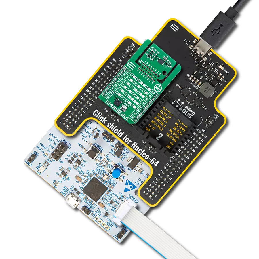
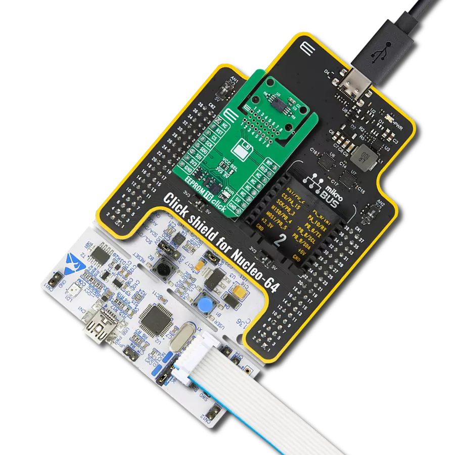
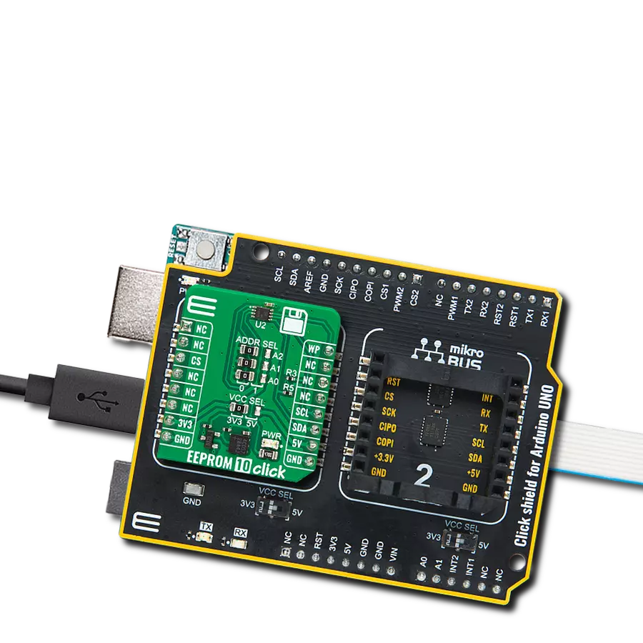
EEPROM 4 Click
Dev. board
EasyAVR v7
Compiler
NECTO Studio
MCU
ATmega644P
Discover a solution that guarantees data retention for extended periods, offering peace of mind in critical scenarios and safeguarding valuable information against unforeseen events
A
A
Hardware Overview
How does it work?
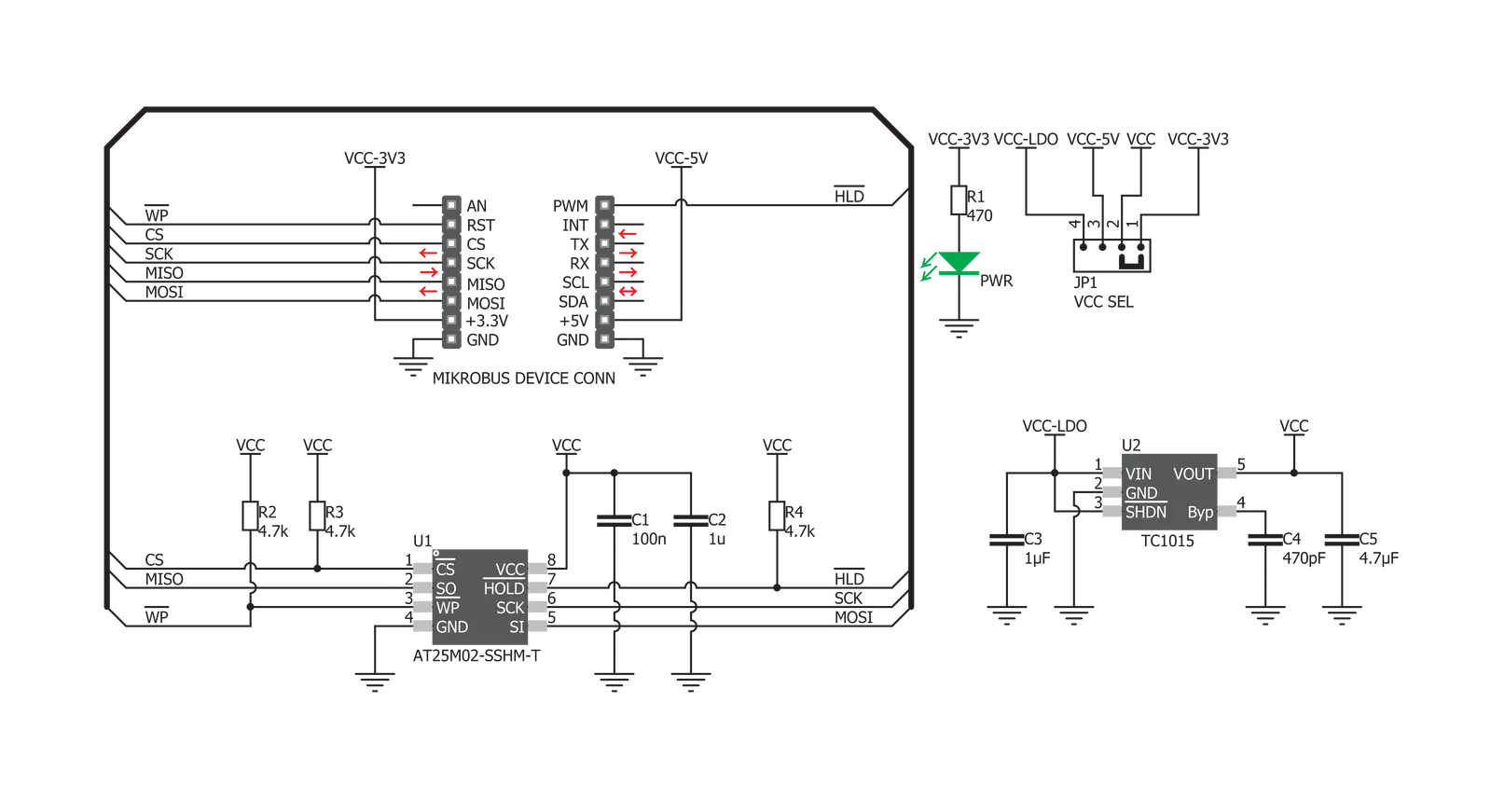
EEPROM 4 Click is based on the AT25M02, an SPI serial EEPROM from Microchip, with a memory cell density of 2 Mbits. The EEPROM density is usually expressed in bits, so exactly 2,097,152 bits are organized in units or words of 8 bits, which gives 262,144 bytes of data memory. Furthermore, the EEPROM is organized into so-called pages. One page holds 256 bytes, and there are 1024 pages (1024 pages x 256 bytes = 262,144 bytes total). Having insight into how the memory cells are organized is important for write and erase operations. The SPI pins are routed to the mikroBUS™, making communication easy and straightforward. The SPI can be clocked as high as 5MHz, providing a fast throughput for the data transfer. A dedicated #HOLD pin is routed to the PWM pin of the mikroBUS™. When the communication with the click board™ is initiated by setting the CS pin to a LOW logic state, it is possible to pause the serial data transfer without
resetting the communication if the #HOLD pin (PWM pin on the mikroBUS™) is set to a LOW logic state. To resume the communication, setting this pin to a HIGH logic state while the SCK is still running is enough. Once the HOLD is initiated, the state of the SCK line is irrelevant, and any serial data input will be ignored. This pin is pulled HIGH by the onboard resistor. A dedicated #WP write protect pin puts the device into the hardware write protect mode. This pin is routed to the RST pin of the mikroBUS™. Hardware write-protect works with the Write Protect Enable (WPEN) bit of the Status Register. When this bit is set to 1, and the #WP pin is set to a LOW logic state, the device will ignore any attempt to write to the Status Register and the EEPROM memory regions selected by the Block Write Protect bits of the Status Register (BP0 and BP1). WRSR instruction is used to write to the Status Register (01h). Again, WREN instruction should be executed first before
attempting to write to Status Register. Once the WPEN bit is set to 1 and the RST has been pulled to a LOW logic state, setting the WPEN bit to 0 won’t turn off write protection as long as the #WP pin (RST) stays LOW. WPEN bit and the BP0 and BP1 bits are constructed as EEPROM cells, meaning that they are nonvolatile and will retain their states even after power is off. The #WP pin is pulled HIGH by the onboard resistor. As usual, the onboard SMD jumper labeled as VCCSEL is used to select the operating voltage between 3.3V and 5V. However, there’s the third position for this jumper, which sets the operating voltage to 1.8V. This is achieved thanks to the TC1015, a small 100 mA LDO from Microchip powered by the 5V rail. As always, MikroElektronika provides libraries that simplify and speed up working with this device. The provided application example demonstrates the functionality of the provided libraries and can be used as a reference point for own development.


Features overview
Development board
EasyAVR v7 is the seventh generation of AVR development boards specially designed for the needs of rapid development of embedded applications. It supports a wide range of 16-bit AVR microcontrollers from Microchip and has a broad set of unique functions, such as a powerful onboard mikroProg programmer and In-Circuit debugger over USB. The development board is well organized and designed so that the end-user has all the necessary elements in one place, such as switches, buttons, indicators, connectors, and others. With four different connectors for each port, EasyAVR v7 allows you to connect accessory boards, sensors, and custom electronics more
efficiently than ever. Each part of the EasyAVR v7 development board contains the components necessary for the most efficient operation of the same board. An integrated mikroProg, a fast USB 2.0 programmer with mikroICD hardware In-Circuit Debugger, offers many valuable programming/debugging options and seamless integration with the Mikroe software environment. Besides it also includes a clean and regulated power supply block for the development board. It can use a wide range of external power sources, including an external 12V power supply, 7-12V AC or 9-15V DC via DC connector/screw terminals, and a power source via the USB Type-B (USB-B)
connector. Communication options such as USB-UART and RS-232 are also included, alongside the well-established mikroBUS™ standard, three display options (7-segment, graphical, and character-based LCD), and several different DIP sockets which cover a wide range of 16-bit AVR MCUs. EasyAVR v7 is an integral part of the Mikroe ecosystem for rapid development. Natively supported by Mikroe software tools, it covers many aspects of prototyping and development thanks to a considerable number of different Click boards™ (over a thousand boards), the number of which is growing every day.

Microcontroller Overview
MCU Card / MCU
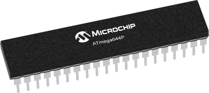
Architecture
AVR
MCU Memory (KB)
64
Silicon Vendor
Microchip
Pin count
40
RAM (Bytes)
4096
Used MCU Pins
mikroBUS™ mapper
Take a closer look
Click board™ Schematic
Step by step
Project assembly

Start by selecting your development board and Click board™. Begin with the EasyAVR v7 as your development board.


Track your results in real time
Application Output
1. Application Output - In Debug mode, the 'Application Output' window enables real-time data monitoring, offering direct insight into execution results. Ensure proper data display by configuring the environment correctly using the provided tutorial.

2. UART Terminal - Use the UART Terminal to monitor data transmission via a USB to UART converter, allowing direct communication between the Click board™ and your development system. Configure the baud rate and other serial settings according to your project's requirements to ensure proper functionality. For step-by-step setup instructions, refer to the provided tutorial.

3. Plot Output - The Plot feature offers a powerful way to visualize real-time sensor data, enabling trend analysis, debugging, and comparison of multiple data points. To set it up correctly, follow the provided tutorial, which includes a step-by-step example of using the Plot feature to display Click board™ readings. To use the Plot feature in your code, use the function: plot(*insert_graph_name*, variable_name);. This is a general format, and it is up to the user to replace 'insert_graph_name' with the actual graph name and 'variable_name' with the parameter to be displayed.

Software Support
Library Description
This library contains API for EEPROM 4 Click driver.
Key functions:
eeprom4_write_status_reg- Status register write functioneeprom4_write_memory- Memory array write functioneeprom4_read_memory- Memory array read function
Open Source
Code example
The complete application code and a ready-to-use project are available through the NECTO Studio Package Manager for direct installation in the NECTO Studio. The application code can also be found on the MIKROE GitHub account.
/*!
 * \file
 * \brief Eeprom4 Click example
 *
 * # Description
 * This Click reads and writes memory.
 *
 * The demo application is composed of two sections :
 *
 * ## Application Init
 * Initializes Click driver and configures Click that all memory block > is unprotected.
 * Also configures that HOLD operation is disabled, and the memory and > status register are writable.
 *
 * ## Application Task
 * Enables writting to memory array, writes data from buffer to memory,
 * checks if the part is in a write cycle, and if is not reads data >  > from memory array and stores data to buffer.
 * Storaged data shows on USB UART.
 *
 * \author MikroE Team
 *
 */
// ------------------------------------------------------------------- INCLUDES

#include "board.h"
#include "log.h"
#include "eeprom4.h"

// ------------------------------------------------------------------ VARIABLES

static eeprom4_t eeprom4;
static log_t logger;

// ------------------------------------------------------ APPLICATION FUNCTIONS

void application_init ( void )
{
    log_cfg_t log_cfg;
    eeprom4_cfg_t cfg;

    /**
     * Logger initialization.
     * Default baud rate: 115200
     * Default log level: LOG_LEVEL_DEBUG
     * @note If USB_UART_RX and USB_UART_TX
     * are defined as HAL_PIN_NC, you will
     * need to define them manually for log to work.
     * See @b LOG_MAP_USB_UART macro definition for detailed explanation.
     */
    LOG_MAP_USB_UART( log_cfg );
    log_init( &logger, &log_cfg );
    log_info( &logger, "---- Application Init ----" );

    //  Click initialization.

    eeprom4_cfg_setup( &cfg );
    EEPROM4_MAP_MIKROBUS( cfg, MIKROBUS_1 );
    eeprom4_init( &eeprom4, &cfg );

    eeprom4_default_cfg( &eeprom4 );
}

void application_task (  )
{
    uint8_t data_write[ 13 ] = { 'M', 'i', 'K', 'r', 'O', 'e', 0 };
    uint8_t data_read[ 255 ] = { 0 };
    uint8_t cnt;
    uint8_t check_state;

    eeprom4_send_command( &eeprom4, EEPROM4_SET_WRITE_ENABLE_LATCH_COMMAND );
    eeprom4_write_memory( &eeprom4, EEPROM4_FIRST_MEMORY_LOCATION, data_write, 6 );

    cnt = eeprom4_check_status_reg( &eeprom4, EEPROM4_READY_BIT );
    check_state = eeprom4_send_command( &eeprom4, EEPROM4_LOW_POWER_WRITE_POLL_COMMAND );

    while ( cnt | check_state )
    {
        cnt = eeprom4_check_status_reg( &eeprom4, EEPROM4_READY_BIT );
        check_state = eeprom4_send_command( &eeprom4, EEPROM4_LOW_POWER_WRITE_POLL_COMMAND );
    }

    eeprom4_read_memory( &eeprom4, 0x00000000, data_read, 6 );

    for ( cnt = 0; cnt < 6; cnt++ )
    {
        log_printf( &logger, " %c ", data_read[cnt] );
    }
    log_printf( &logger, "-----   \r\n" );

    Delay_ms ( 1000 );
    Delay_ms ( 1000 );
}

int main ( void )
{
    /* Do not remove this line or clock might not be set correctly. */
    #ifdef PREINIT_SUPPORTED
    preinit();
    #endif

    application_init( );

    for ( ; ; )
    {
        application_task( );
    }

    return 0;
}


// ------------------------------------------------------------------------ END