Accelerate data access and retrieval like never before with W25Q128JV and ATmega644P
Flash forward to excellence

Published Aug 28, 2023
Click board™
Flash 6 Click
Dev. board
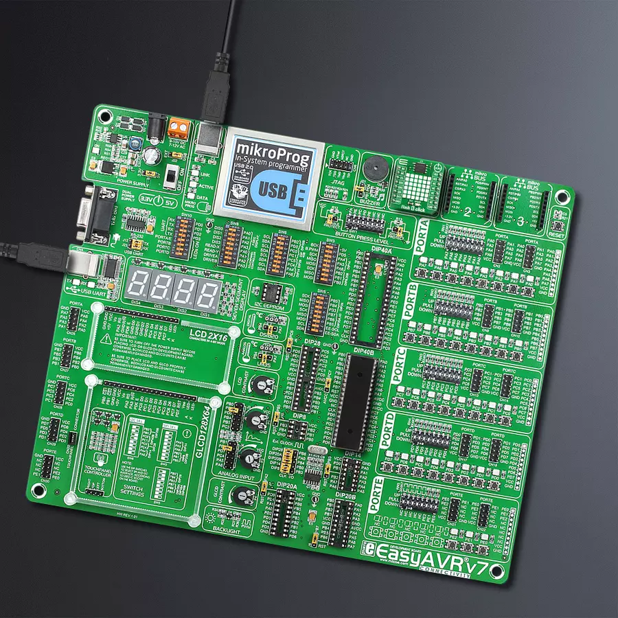
EasyAVR v7
Compiler
NECTO Studio
MCU
ATmega644P
Upgrade to faster, reliable storage with our flash memory solution
A
A
Hardware Overview
How does it work?
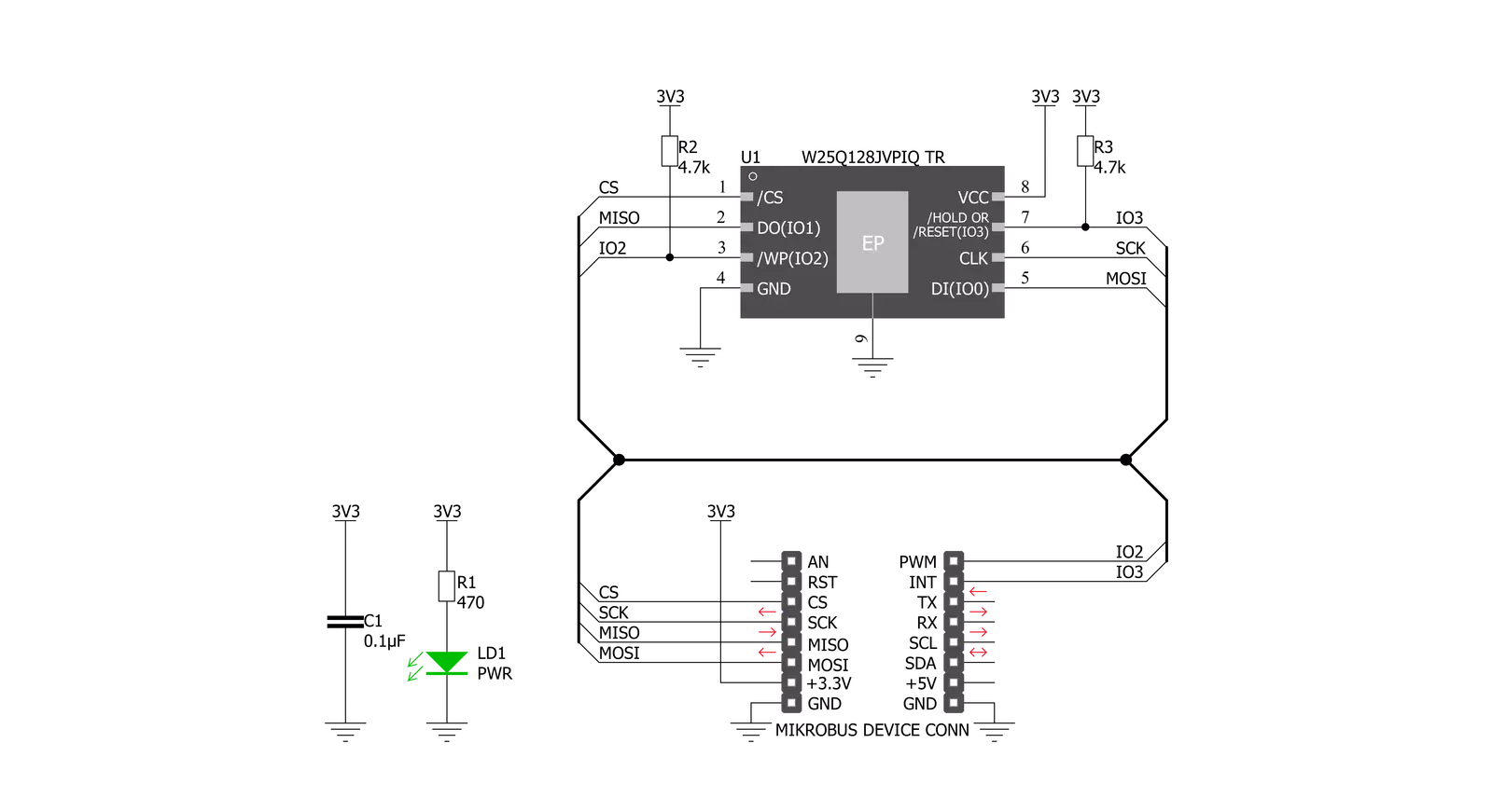
Flash 6 Click is based on the W25Q128JV, a 128M-bit flash memory from Winbond organized into 65,536 programmable pages of 256 bytes each. Up to 256 bytes can be programmed at a time. Pages can be erased in groups of 16 (4KB sector erase), groups of 128 (32KB block erase), groups of 256 (64KB block erase), or the entire chip (chip erase). The W25Q128JV has 4,096 erasable sectors and 256 erasable blocks respectively. The small 4KB sectors allow for greater flexibility in applications that require data and parameter storage. The Flash 6 Click uses the standard Serial Peripheral Interface (SPI), supporting SPI clock frequencies of up to 133MHz Single, Dual/Quad SPI clocks. Besides that, the W25Q128JV provides a Continuous Read Mode that allows for efficient access to the entire memory array with a single Read command. This feature is ideal for
code-shadowing applications. Also, it offers the highest performance thanks to 133MHz Standard/Dual/Quad SPI clocks and a 66MB/S continuous data transfer rate. It has an efficient Continuous Read Mode, allowing direct read access to the entire array. However, the performance depends on the main MCU used with this Click board™. A Hold pin, Write Protect pin and programmable write protection provide further control flexibility. Additionally, the device supports JEDEC standard manufacturer and device ID and SFDP, a 64-bit Unique Serial Number, and three 256-byte Security Registers. The W25Q128JV is accessed through an SPI-compatible bus consisting of four signals: Serial Clock (CLK), Chip Select (/CS), Serial Data Input (DI), and Serial Data Output (DO). Standard SPI instructions use the DI input pin to serially
write instructions, addresses, or data to the device on the rising edge of CLK. The DO output pin reads data or status from the device on the falling edge of CLK. For a detailed explanation, please consult the included datasheet. However, MIKROE provides a library that contains functions that simplify and speed up working with this device. The provided application example demonstrates the functionality of the library functions. It can be used as a reference for a custom project development. This Click board™ can be operated only with a 3.3V logic voltage level. The board must perform appropriate logic voltage level conversion before using MCUs with different logic levels. Also, it comes equipped with a library containing functions and an example code that can be used as a reference for further development.


Features overview
Development board
EasyAVR v7 is the seventh generation of AVR development boards specially designed for the needs of rapid development of embedded applications. It supports a wide range of 16-bit AVR microcontrollers from Microchip and has a broad set of unique functions, such as a powerful onboard mikroProg programmer and In-Circuit debugger over USB. The development board is well organized and designed so that the end-user has all the necessary elements in one place, such as switches, buttons, indicators, connectors, and others. With four different connectors for each port, EasyAVR v7 allows you to connect accessory boards, sensors, and custom electronics more
efficiently than ever. Each part of the EasyAVR v7 development board contains the components necessary for the most efficient operation of the same board. An integrated mikroProg, a fast USB 2.0 programmer with mikroICD hardware In-Circuit Debugger, offers many valuable programming/debugging options and seamless integration with the Mikroe software environment. Besides it also includes a clean and regulated power supply block for the development board. It can use a wide range of external power sources, including an external 12V power supply, 7-12V AC or 9-15V DC via DC connector/screw terminals, and a power source via the USB Type-B (USB-B)
connector. Communication options such as USB-UART and RS-232 are also included, alongside the well-established mikroBUS™ standard, three display options (7-segment, graphical, and character-based LCD), and several different DIP sockets which cover a wide range of 16-bit AVR MCUs. EasyAVR v7 is an integral part of the Mikroe ecosystem for rapid development. Natively supported by Mikroe software tools, it covers many aspects of prototyping and development thanks to a considerable number of different Click boards™ (over a thousand boards), the number of which is growing every day.

Microcontroller Overview
MCU Card / MCU
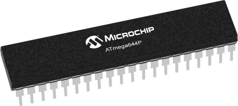
Architecture
AVR
MCU Memory (KB)
64
Silicon Vendor
Microchip
Pin count
40
RAM (Bytes)
4096
Used MCU Pins
mikroBUS™ mapper
Take a closer look
Click board™ Schematic
Step by step
Project assembly

Start by selecting your development board and Click board™. Begin with the EasyAVR v7 as your development board.


Track your results in real time
Application Output
1. Application Output - In Debug mode, the 'Application Output' window enables real-time data monitoring, offering direct insight into execution results. Ensure proper data display by configuring the environment correctly using the provided tutorial.

2. UART Terminal - Use the UART Terminal to monitor data transmission via a USB to UART converter, allowing direct communication between the Click board™ and your development system. Configure the baud rate and other serial settings according to your project's requirements to ensure proper functionality. For step-by-step setup instructions, refer to the provided tutorial.

3. Plot Output - The Plot feature offers a powerful way to visualize real-time sensor data, enabling trend analysis, debugging, and comparison of multiple data points. To set it up correctly, follow the provided tutorial, which includes a step-by-step example of using the Plot feature to display Click board™ readings. To use the Plot feature in your code, use the function: plot(*insert_graph_name*, variable_name);. This is a general format, and it is up to the user to replace 'insert_graph_name' with the actual graph name and 'variable_name' with the parameter to be displayed.

Software Support
Library Description
This library contains API for Flash 6 Click driver.
Key functions:
flash6_write_memory_data- Function used for writing in memoryflash6_read_memory_data- Function used for reading from memoryflash6_erase_memory_segment- Function for eraseing segment
Open Source
Code example
The complete application code and a ready-to-use project are available through the NECTO Studio Package Manager for direct installation in the NECTO Studio. The application code can also be found on the MIKROE GitHub account.
/*!
 * \file
 * \brief Flash6 Click example
 *
 * # Description
 * This application writes in memory and reads from memory.
 *
 * The demo application is composed of two sections :
 *
 * ## Application Init
 * Initializes driver, resets device and tests communication.
 *
 * ## Application Task
 * Clears the memory sector, writes "MikroE" to device memory
 * and then reads it and sends it to log every 2 sec.
 *
 * \author MikroE Team
 *
 */
// ------------------------------------------------------------------- INCLUDES

#include "board.h"
#include "log.h"
#include "flash6.h"

// ------------------------------------------------------------------ VARIABLES

static flash6_t flash6;
static log_t logger;

static char write_buf[ 9 ] = { 'M', 'i', 'k', 'r', 'o', 'E', 13, 10, 0 };

// ------------------------------------------------------ APPLICATION FUNCTIONS

void application_init ( void )
{
    log_cfg_t log_cfg;
    flash6_cfg_t cfg;

    uint8_t manufacture_id;
    uint8_t device_id;

    /**
     * Logger initialization.
     * Default baud rate: 115200
     * Default log level: LOG_LEVEL_DEBUG
     * @note If USB_UART_RX and USB_UART_TX
     * are defined as HAL_PIN_NC, you will
     * need to define them manually for log to work.
     * See @b LOG_MAP_USB_UART macro definition for detailed explanation.
     */
    LOG_MAP_USB_UART( log_cfg );
    log_init( &logger, &log_cfg );
    log_info( &logger, "---- Application Init ----" );

    //  Click initialization.

    flash6_cfg_setup( &cfg );
    FLASH6_MAP_MIKROBUS( cfg, MIKROBUS_1 );
    flash6_init( &flash6, &cfg );

    flash6_software_reset( &flash6 );
    Delay_ms ( 100 );

    flash6_get_manufacture_device_id( &flash6, &manufacture_id, &device_id );
    log_printf( &logger, "\r\n ------> MANUFACTURE ID: 0x%x \r\n", manufacture_id );
    log_printf( &logger, " ------> DEVICE ID: 0x%x \r\n \r\n", device_id );
    Delay_ms ( 1000 );
}

void application_task ( void )
{
    uint32_t start_addr;
    char read_buff[ 50 ];
    uint8_t cnt;

    start_addr = 0x002000;

    log_printf( &logger, " ---> Erase sector  \r\n" );
    flash6_erase_memory_segment( &flash6, FLASH6_CMD_SECTOR_ERASE_4KB, start_addr );
    Delay_ms ( 500 );

    log_printf( &logger, " ---> Write in memory ... \r\n" );
    flash6_write_memory_data( &flash6, start_addr, &write_buf[ 0 ], 9 );
    log_printf( &logger, " ---> Read from memory \r\n" );
    flash6_read_memory_data( &flash6, start_addr, read_buff, 9 );

    log_printf( &logger, "---->>>> " );

    log_printf( &logger, "%s ", read_buff );
    Delay_ms ( 100 );
    log_printf( &logger, "----------------------------------\r\n" );

    Delay_ms ( 1000 );
    Delay_ms ( 1000 );
}

int main ( void )
{
    /* Do not remove this line or clock might not be set correctly. */
    #ifdef PREINIT_SUPPORTED
    preinit();
    #endif

    application_init( );

    for ( ; ; )
    {
        application_task( );
    }

    return 0;
}

// ------------------------------------------------------------------------ END