Experience the seamless blend of capacity and velocity with AT25SF321B and PIC32MZ1024EFH064
Flash forward: Upgrade storage, empower innovation

Published Nov 11, 2023
Click board™
Flash 11 Click
Dev. board
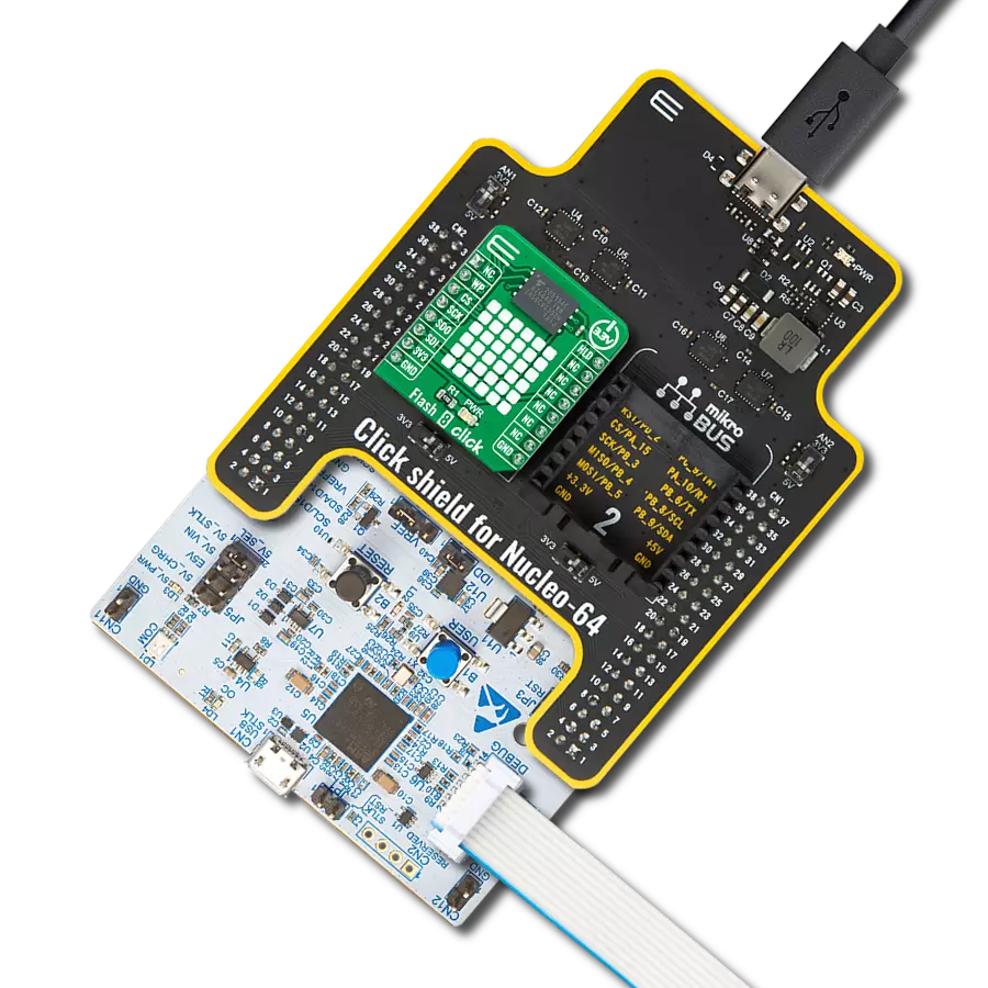
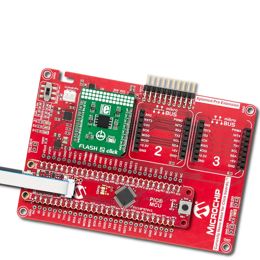
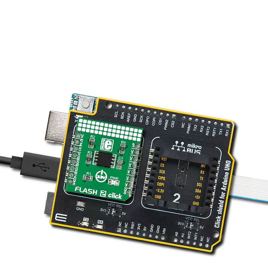
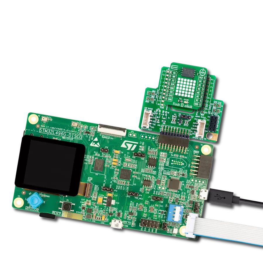
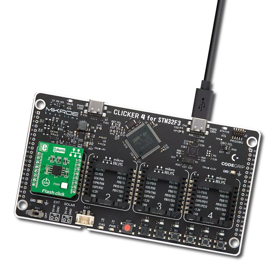
PIC32MZ clicker
Compiler
NECTO Studio
MCU
PIC32MZ1024EFH064
Data management reaches new heights with our flash memory marvel.
A
A
Hardware Overview
How does it work?
Flash 11 Click is based on the AT25SF321B, a 32-Mbit SPI serial Flash memory with Dual I/O and Quad I/O support from Dialog Semiconductor. The AT25SF321A is organized as a 32Mbit (4Mx8 physical block) Flash memory where the memory array can be erased in four levels of granularity, including a full-chip erase, which, depending on the blocks, can be done typically in 10 seconds. In addition, the optimized erase architecture allows erasing data in 4kB, 32kB, and 64kB block erase operations. Optimizing the erase blocks' size can be the most efficient use of memory space. The AT25SF321B specifies a minimum of 100.000 endurance cycles with data retention of a minimum of 20 years, allowing it to handle (almost) unlimited reads/writes to the memory. Flash 11 Click communicates with MCU through a
standard SPI interface supporting the two most common SPI modes, SPI Mode 0 and 3, and a maximum clock frequency of up to 108MHz. Furthermore, this Click board™ provides additional hardware-controlled functions. The configurable Write Protection, marked as WP and routed on the default position of the PWM pin of the mikroBUS™ socket, protects all registers (including status and configuration) from write operations and must be held low to inhibit all the write operations to registers. When this pin is in a low logic state, all memory and register write are prohibited, and the address count is not incremented. In addition, there is software write protection too. Also, it is possible to use the Reset or Hold function through the RST pin of the mikroBUS™ socket, depending on the state of the
HOLD/RESET bit 7 in Status Register 3. In the case of the Hold function, this pin temporarily pauses serial communication without deselecting or resetting the device, while in the case of the Reset feature, a low logic level on the RST pin puts the AT25SF321B into a Reset state. This is a part of the Program and Erase, Suspend, and Resume features of the Flash 11 Click. This Click board™ can be operated only with a 3.3V logic voltage level. The board must perform appropriate logic voltage level conversion before using MCUs with different logic levels. Also, it comes equipped with a library containing functions and an example code that can be used as a reference for further development.

Features overview
Development board
PIC32MZ Clicker is a compact starter development board that brings the flexibility of add-on Click boards™ to your favorite microcontroller, making it a perfect starter kit for implementing your ideas. It comes with an onboard 32-bit PIC32MZ microcontroller with FPU from Microchip, a USB connector, LED indicators, buttons, a mikroProg connector, and a header for interfacing with external electronics. Thanks to its compact design with clear and easy-recognizable silkscreen markings, it provides a fluid and immersive working experience, allowing access anywhere and under
any circumstances. Each part of the PIC32MZ Clicker development kit contains the components necessary for the most efficient operation of the same board. In addition to the possibility of choosing the PIC32MZ Clicker programming method, using USB HID mikroBootloader, or through an external mikroProg connector for PIC, dsPIC, or PIC32 programmer, the Clicker board also includes a clean and regulated power supply module for the development kit. The USB Micro-B connection can provide up to 500mA of current, which is more than enough to operate all onboard
and additional modules. All communication methods that mikroBUS™ itself supports are on this board, including the well-established mikroBUS™ socket, reset button, and several buttons and LED indicators. PIC32MZ Clicker is an integral part of the Mikroe ecosystem, allowing you to create a new application in minutes. Natively supported by Mikroe software tools, it covers many aspects of prototyping thanks to a considerable number of different Click boards™ (over a thousand boards), the number of which is growing every day.

Microcontroller Overview
MCU Card / MCU
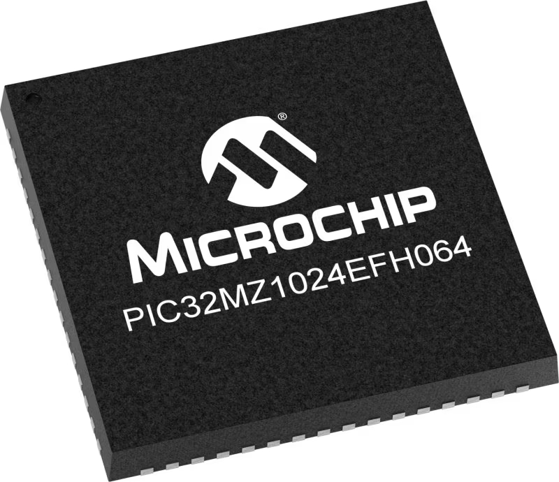
Architecture
PIC32
MCU Memory (KB)
1024
Silicon Vendor
Microchip
Pin count
64
RAM (Bytes)
524288
Used MCU Pins
mikroBUS™ mapper
Take a closer look
Click board™ Schematic

Step by step
Project assembly

Start by selecting your development board and Click board™. Begin with the PIC32MZ clicker as your development board.


Track your results in real time
Application Output
1. Application Output - In Debug mode, the 'Application Output' window enables real-time data monitoring, offering direct insight into execution results. Ensure proper data display by configuring the environment correctly using the provided tutorial.

2. UART Terminal - Use the UART Terminal to monitor data transmission via a USB to UART converter, allowing direct communication between the Click board™ and your development system. Configure the baud rate and other serial settings according to your project's requirements to ensure proper functionality. For step-by-step setup instructions, refer to the provided tutorial.

3. Plot Output - The Plot feature offers a powerful way to visualize real-time sensor data, enabling trend analysis, debugging, and comparison of multiple data points. To set it up correctly, follow the provided tutorial, which includes a step-by-step example of using the Plot feature to display Click board™ readings. To use the Plot feature in your code, use the function: plot(*insert_graph_name*, variable_name);. This is a general format, and it is up to the user to replace 'insert_graph_name' with the actual graph name and 'variable_name' with the parameter to be displayed.

Software Support
Library Description
This library contains API for Flash 11 Click driver.
Key functions:
flash11_memory_write- Flash 11 memory write function.flash11_memory_read- Flash 11 memory read function.flash11_block_erase- Flash 11 block erase function.
Open Source
Code example
The complete application code and a ready-to-use project are available through the NECTO Studio Package Manager for direct installation in the NECTO Studio. The application code can also be found on the MIKROE GitHub account.
/*!
 * @file main.c
 * @brief Flash 11 Click example
 *
 * # Description
 * This example demonstrates the use of Flash 11 Click board.
 * The demo app writes specified data to the memory and reads it back.
 *
 * The demo application is composed of two sections :
 *
 * ## Application Init
 * The initialization of SPI module, log UART, and additional pins.
 * After the driver init, the app executes a default configuration.
 *
 * ## Application Task
 * This example demonstrates the use of the Flash 11 Click board™.
 * The demo application writes a desired number of bytes to the memory
 * and then verifies if it is written correctly
 * by reading from the same memory location and displaying the memory content.
 * Results are being sent to the UART Terminal, where you can track their changes.
 *
 * @author Nenad Filipovic
 *
 */

#include "board.h"
#include "log.h"
#include "flash11.h"

static flash11_t flash11;
static log_t logger;

#define DEMO_TEXT_MESSAGE_1         "MikroE"
#define STARTING_ADDRESS_1           0x010203ul
#define DEMO_TEXT_MESSAGE_2         "Flash 11 Click"
#define STARTING_ADDRESS_2           0x123456ul

void application_init ( void )
{
    log_cfg_t log_cfg;  /**< Logger config object. */
    flash11_cfg_t flash11_cfg;  /**< Click config object. */

    /**
     * Logger initialization.
     * Default baud rate: 115200
     * Default log level: LOG_LEVEL_DEBUG
     * @note If USB_UART_RX and USB_UART_TX
     * are defined as HAL_PIN_NC, you will
     * need to define them manually for log to work.
     * See @b LOG_MAP_USB_UART macro definition for detailed explanation.
     */
    LOG_MAP_USB_UART( log_cfg );
    log_init( &logger, &log_cfg );
    log_info( &logger, " Application Init " );

    // Click initialization.
    flash11_cfg_setup( &flash11_cfg );
    FLASH11_MAP_MIKROBUS( flash11_cfg, MIKROBUS_1 );
    if ( SPI_MASTER_ERROR == flash11_init( &flash11, &flash11_cfg ) )
    {
        log_error( &logger, " Communication init." );
        for ( ; ; );
    }

    if ( FLASH11_ERROR == flash11_default_cfg ( &flash11 ) )
    {
        log_error( &logger, " Default configuration." );
        for ( ; ; );
    }

    log_info( &logger, " Application Task " );
    log_printf( &logger, " ----------------------------\r\n" );
    Delay_ms ( 100 );
}

void application_task ( void )
{
    uint8_t data_buf[ 128 ] = { 0 };
    log_printf( &logger, " Memory address: 0x%.6LX\r\n", ( uint32_t ) STARTING_ADDRESS_1 );
    if ( FLASH11_OK == flash11_block_erase( &flash11, FLASH11_CMD_BLOCK_ERASE_4KB, STARTING_ADDRESS_1 ) )
    {
        log_printf( &logger, " Erase memory block (4KB)\r\n" );
    }

    memcpy( data_buf, DEMO_TEXT_MESSAGE_1, strlen( DEMO_TEXT_MESSAGE_1 ) );
    if ( FLASH11_OK == flash11_memory_write( &flash11, STARTING_ADDRESS_1, data_buf, sizeof( data_buf ) ) )
    {
        log_printf( &logger, " Write data: %s\r\n", data_buf );
        Delay_ms ( 100 );
    }

    memset( data_buf, 0, sizeof( data_buf ) );
    if ( FLASH11_OK == flash11_memory_read( &flash11, STARTING_ADDRESS_1, data_buf, sizeof( data_buf ) ) )
    {
        log_printf( &logger, " Read data: %s\r\n", data_buf );
        Delay_ms ( 1000 );
        Delay_ms ( 1000 );
        Delay_ms ( 1000 );
    }
    log_printf( &logger, " ----------------------------\r\n" );

    log_printf( &logger, " Memory address: 0x%.6LX\r\n", ( uint32_t ) STARTING_ADDRESS_2 );
    if ( FLASH11_OK == flash11_block_erase( &flash11, FLASH11_CMD_BLOCK_ERASE_4KB, STARTING_ADDRESS_2 ) )
    {
        log_printf( &logger, " Erase memory block (4KB)\r\n" );
    }

    memcpy( data_buf, DEMO_TEXT_MESSAGE_2, strlen( DEMO_TEXT_MESSAGE_2 ) );
    if ( FLASH11_OK == flash11_memory_write( &flash11, STARTING_ADDRESS_2, data_buf, sizeof( data_buf ) ) )
    {
        log_printf( &logger, " Write data: %s\r\n", data_buf );
        Delay_ms ( 100 );
    }

    memset( data_buf, 0, sizeof( data_buf ) );
    if ( FLASH11_OK == flash11_memory_read( &flash11, STARTING_ADDRESS_2, data_buf, sizeof( data_buf ) ) )
    {
        log_printf( &logger, " Read data: %s\r\n", data_buf );
        Delay_ms ( 1000 );
        Delay_ms ( 1000 );
        Delay_ms ( 1000 );
    }
    log_printf ( &logger, " ----------------------------\r\n" );
}

int main ( void )
{
    /* Do not remove this line or clock might not be set correctly. */
    #ifdef PREINIT_SUPPORTED
    preinit();
    #endif

    application_init( );

    for ( ; ; )
    {
        application_task( );
    }

    return 0;
}

// ------------------------------------------------------------------------ END