Translate industrial input signals into serialized SPI-compatible output with MAX22199 and MK64FN1M0VDC12
IEC 61131-2 compliant octal digital input solution for multiple signal types commonly found in industrial settings

Published Apr 16, 2024
Click board™
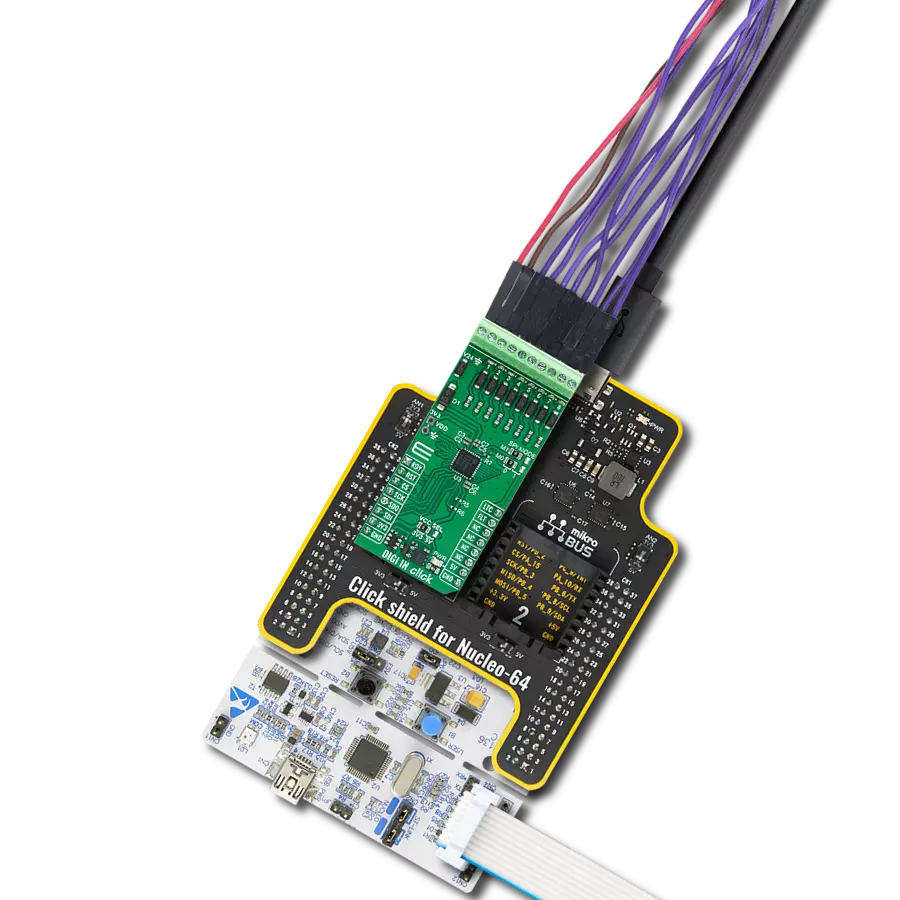
DIGI IN Click
Dev. board
Clicker 2 for Kinetis
Compiler
NECTO Studio
MCU
MK64FN1M0VDC12
Enhance industrial systems with reliable signal processing for precise control and diagnostics in building automation, motor control, and PLCs, boosting reliability and efficiency
A
A
Hardware Overview
How does it work?
DIGI IN Click is based on the MAX22199, an octal industrial digital input module from Analog Devices. The MAX22199 complies with the IEC 61131-2 standard for industrial digital input devices. It efficiently converts eight 7-24V current-sinking industrial inputs into a serialized output compatible with SPI, supporting both 3V and 5V logic systems. It can function as eight Type 1 / Type 3 digital inputs or four Type 2 digital inputs. The eight yellow LEDs, numbered 1 through 8, provide immediate visual feedback on the status of the digital input channels, whether active or not. This Click board™ is designed for various applications, including programmable logic controllers, distributed control systems, motor control applications, and building automation systems. To ensure reliability in the demanding conditions of industrial environments, the MAX22199 incorporates a customizable glitch filter for each input, with noise filters that can be
independently set to any of eight durations ranging from 50µs to 20ms or completely bypassed. A 4-pin SPI interface and an LTC latch input facilitate the device's connectivity, allowing synchronized data sampling across multiple devices. In addition, the MAX22199 is equipped with several diagnostic features, including protection against thermal overload, alarms for under voltage and missing voltage conditions on the 24V supply, and detection mechanisms for SPI and CRC communication errors. These errors can trigger an interrupt signal via the FLT pin. Besides these pins, the mikroBUS™ socket also includes a READY (RDY) pin, which signals when the MAX22199 is operational by transitioning to a LOW state. An additional feature of the board is the provision of SPI MODE jumpers, which offer control over the SPI Mode settings from 0 to 3. Adjusting the M1 jumper to position 1 activates the SPI daisy-chain
mode, whereas setting the M0 jumper to position 1 turns off the CRC error detection feature. The device is powered by a single 7V to 24V supply connected to the V24 terminal. It also includes an integrated LDO regulator that not only powers the MAX22199 but also provides a 3.3V output capable of delivering up to 25mA to external circuits. It should be noted that if this pin is used as a supply of the MAX22199, no power supply should be connected to the V24 terminal. This Click board™ can operate with either 3.3V or 5V logic voltage levels selected via the VCC SEL jumper. This way, both 3.3V and 5V capable MCUs can use the communication lines properly. Also, this Click board™ comes equipped with a library containing easy-to-use functions and an example code that can be used as a reference for further development.

Features overview
Development board
Clicker 2 for Kinetis is a compact starter development board that brings the flexibility of add-on Click boards™ to your favorite microcontroller, making it a perfect starter kit for implementing your ideas. It comes with an onboard 32-bit ARM Cortex-M4F microcontroller, the MK64FN1M0VDC12 from NXP Semiconductors, two mikroBUS™ sockets for Click board™ connectivity, a USB connector, LED indicators, buttons, a JTAG programmer connector, and two 26-pin headers for interfacing with external electronics. Its compact design with clear and easily recognizable silkscreen markings allows you to build gadgets with unique functionalities and
features quickly. Each part of the Clicker 2 for Kinetis development kit contains the components necessary for the most efficient operation of the same board. In addition to the possibility of choosing the Clicker 2 for Kinetis programming method, using a USB HID mikroBootloader or an external mikroProg connector for Kinetis programmer, the Clicker 2 board also includes a clean and regulated power supply module for the development kit. It provides two ways of board-powering; through the USB Micro-B cable, where onboard voltage regulators provide the appropriate voltage levels to each component on the board, or
using a Li-Polymer battery via an onboard battery connector. All communication methods that mikroBUS™ itself supports are on this board, including the well-established mikroBUS™ socket, reset button, and several user-configurable buttons and LED indicators. Clicker 2 for Kinetis is an integral part of the Mikroe ecosystem, allowing you to create a new application in minutes. Natively supported by Mikroe software tools, it covers many aspects of prototyping thanks to a considerable number of different Click boards™ (over a thousand boards), the number of which is growing every day.

Microcontroller Overview
MCU Card / MCU

Architecture
ARM Cortex-M4
MCU Memory (KB)
1024
Silicon Vendor
NXP
Pin count
121
RAM (Bytes)
262144
Used MCU Pins
mikroBUS™ mapper
Take a closer look
Click board™ Schematic

Step by step
Project assembly

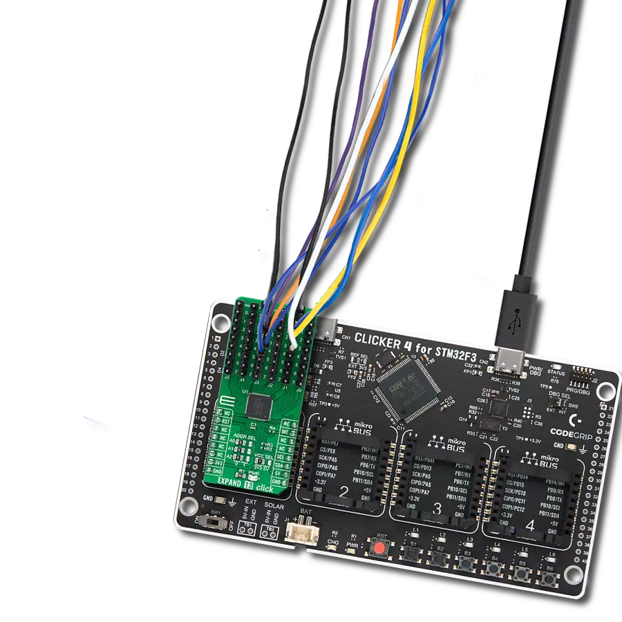
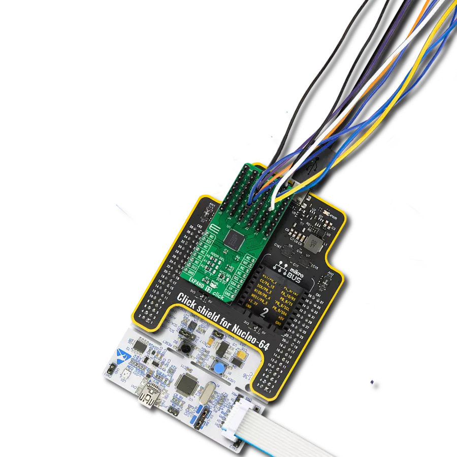
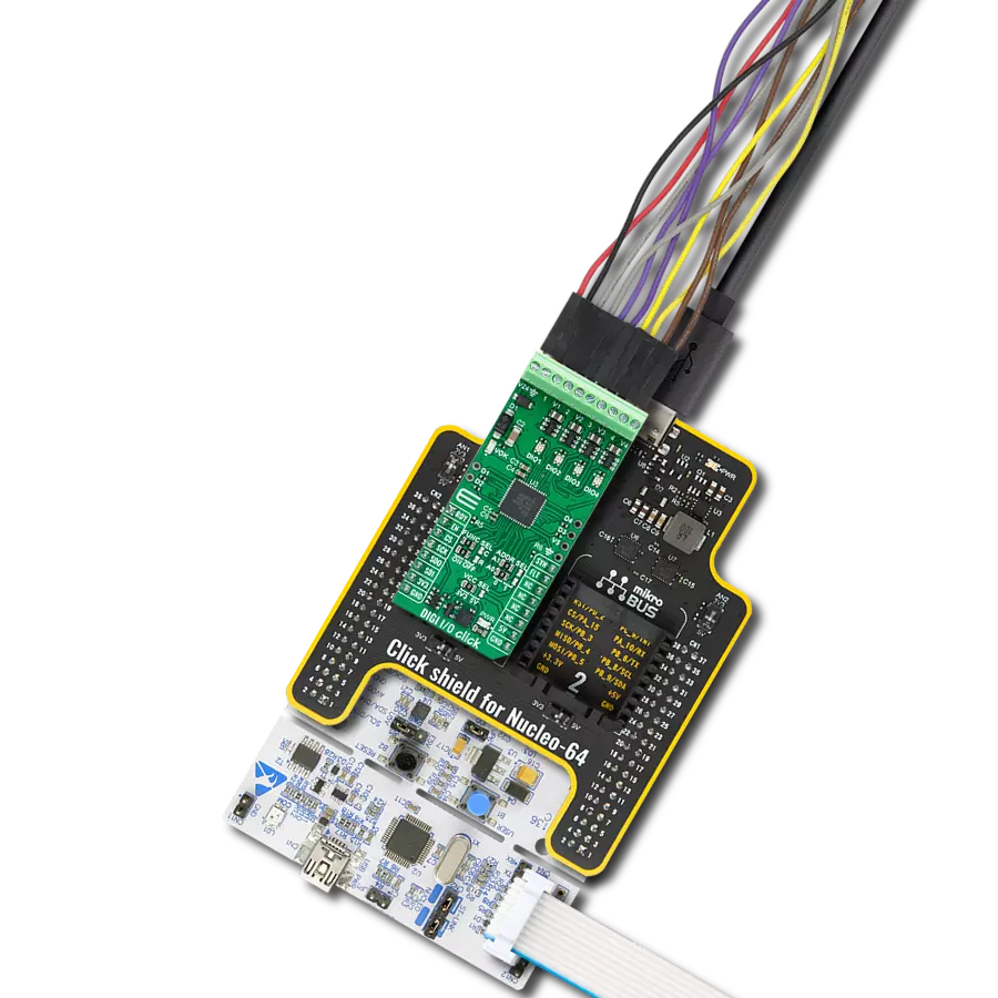
Start by selecting your development board and Click board™. Begin with the Clicker 2 for Kinetis as your development board.


Track your results in real time
Application Output
1. Application Output - In Debug mode, the 'Application Output' window enables real-time data monitoring, offering direct insight into execution results. Ensure proper data display by configuring the environment correctly using the provided tutorial.

2. UART Terminal - Use the UART Terminal to monitor data transmission via a USB to UART converter, allowing direct communication between the Click board™ and your development system. Configure the baud rate and other serial settings according to your project's requirements to ensure proper functionality. For step-by-step setup instructions, refer to the provided tutorial.

3. Plot Output - The Plot feature offers a powerful way to visualize real-time sensor data, enabling trend analysis, debugging, and comparison of multiple data points. To set it up correctly, follow the provided tutorial, which includes a step-by-step example of using the Plot feature to display Click board™ readings. To use the Plot feature in your code, use the function: plot(*insert_graph_name*, variable_name);. This is a general format, and it is up to the user to replace 'insert_graph_name' with the actual graph name and 'variable_name' with the parameter to be displayed.

Software Support
Library Description
This library contains API for DIGI IN Click driver.
Key functions:
digiin_write_reg- This function is used to write data into the selected register by using SPI serial interfacedigiin_read_reg- This function reads a data byte from the selected register by using SPI serial interfacedigiin_pulse_latch- This function is used to generate LATCH pulse for capturing channel data
Open Source
Code example
The complete application code and a ready-to-use project are available through the NECTO Studio Package Manager for direct installation in the NECTO Studio. The application code can also be found on the MIKROE GitHub account.
/*!
 * @file main.c
 * @brief DIGI IN Click example
 *
 * # Description
 * This example demonstrates the use of DIGI IN Click board by reading and
 * displaying the state of the channels.
 *
 * The demo application is composed of two sections :
 *
 * ## Application Init
 * Initializes the driver, performs the Click default configuration.
 *
 * ## Application Task
 * Reads and displays on the USB UART the channel state every second.
 *
 * @author Stefan Ilic
 *
 */

#include "board.h"
#include "log.h"
#include "digiin.h"

static digiin_t digiin;
static log_t logger;

void application_init ( void )
{
    log_cfg_t log_cfg;  /**< Logger config object. */
    digiin_cfg_t digiin_cfg;  /**< Click config object. */

    /**
     * Logger initialization.
     * Default baud rate: 115200
     * Default log level: LOG_LEVEL_DEBUG
     * @note If USB_UART_RX and USB_UART_TX
     * are defined as HAL_PIN_NC, you will
     * need to define them manually for log to work.
     * See @b LOG_MAP_USB_UART macro definition for detailed explanation.
     */
    LOG_MAP_USB_UART( log_cfg );
    log_init( &logger, &log_cfg );
    log_info( &logger, " Application Init " );

    // Click initialization.
    digiin_cfg_setup( &digiin_cfg );
    DIGIIN_MAP_MIKROBUS( digiin_cfg, MIKROBUS_1 );
    if ( SPI_MASTER_ERROR == digiin_init( &digiin, &digiin_cfg ) )
    {
        log_error( &logger, " Communication init." );
        for ( ; ; );
    }

    while ( DIGIIN_PIN_STATE_HIGH == digiin_get_rdy_pin( &digiin ) )
    {
        log_printf( &logger, "Please check if 24V is connected \r\n" );
        Delay_ms ( 1000 );
    }

    if ( DIGIIN_ERROR == digiin_default_cfg ( &digiin ) )
    {
        log_error( &logger, " Default configuration." );
        for ( ; ; );
    }

    log_info( &logger, " Application Task " );
}

void application_task ( void )
{
    uint8_t channel_data = 0;

    digiin_pulse_latch( &digiin );

    if ( DIGIIN_OK == digiin_read_reg( &digiin, DIGIIN_REG_DISTATE, &channel_data ) )
    {
        if ( channel_data & DIGIIN_CHANNEL_1_MASK )
        {
            log_printf( &logger, "Channel 1 State: HIGH \r\n" );
        }
        else
        {
            log_printf( &logger, "Channel 1 State: LOW \r\n" );
        }
        if ( channel_data & DIGIIN_CHANNEL_2_MASK )
        {
            log_printf( &logger, "Channel 2 State: HIGH \r\n" );
        }
        else
        {
            log_printf( &logger, "Channel 2 State: LOW \r\n" );
        }
        if ( channel_data & DIGIIN_CHANNEL_3_MASK )
        {
            log_printf( &logger, "Channel 3 State: HIGH \r\n" );
        }
        else
        {
            log_printf( &logger, "Channel 3 State: LOW \r\n" );
        }
        if ( channel_data & DIGIIN_CHANNEL_4_MASK )
        {
            log_printf( &logger, "Channel 4 State: HIGH \r\n" );
        }
        else
        {
            log_printf( &logger, "Channel 4 State: LOW \r\n" );
        }
        if ( channel_data & DIGIIN_CHANNEL_5_MASK )
        {
            log_printf( &logger, "Channel 5 State: HIGH \r\n" );
        }
        else
        {
            log_printf( &logger, "Channel 5 State: LOW \r\n" );
        }
        if ( channel_data & DIGIIN_CHANNEL_6_MASK )
        {
            log_printf( &logger, "Channel 6 State: HIGH \r\n" );
        }
        else
        {
            log_printf( &logger, "Channel 6 State: LOW \r\n" );
        }
        if ( channel_data & DIGIIN_CHANNEL_7_MASK )
        {
            log_printf( &logger, "Channel 7 State: HIGH \r\n" );
        }
        else
        {
            log_printf( &logger, "Channel 7 State: LOW \r\n" );
        }
        if ( channel_data & DIGIIN_CHANNEL_8_MASK )
        {
            log_printf( &logger, "Channel 8 State: HIGH \r\n" );
        }
        else
        {
            log_printf( &logger, "Channel 8 State: LOW \r\n" );
        }
        log_printf( &logger, "- - - - - - - - - - - - - -\r\n" );
    }
    if ( DIGIIN_PIN_STATE_LOW == digiin_get_flt_pin( &digiin ) )
    {
        uint8_t flt_data = 0;
        digiin_read_reg( &digiin, DIGIIN_REG_FAULT1, &flt_data );
        log_printf( &logger, "Fault1 data: 0x%.2X \r\n", ( uint16_t ) flt_data );
        digiin_read_reg( &digiin, DIGIIN_REG_FAULT2, &flt_data );
        log_printf( &logger, "Fault2 data: 0x%.2X \r\n", ( uint16_t ) flt_data );
        log_printf( &logger, "- - - - - - - - - - - - - -\r\n" );
    }

    Delay_ms ( 1000 );
}

int main ( void )
{
    /* Do not remove this line or clock might not be set correctly. */
    #ifdef PREINIT_SUPPORTED
    preinit();
    #endif

    application_init( );

    for ( ; ; )
    {
        application_task( );
    }

    return 0;
}

// ------------------------------------------------------------------------ END