Decode, express, and amplify data across diverse applications with MCP4728 and MK64FN1M0VDC12
Empower data expression

Published Aug 18, 2023
Click board™
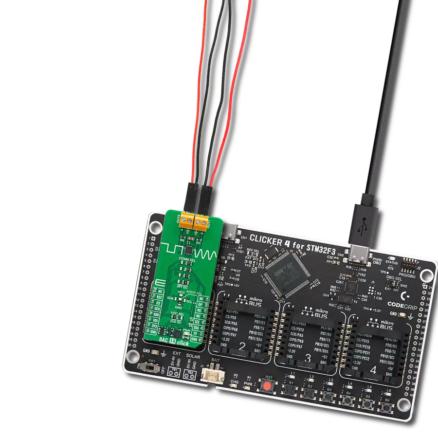
DAC 4 Click
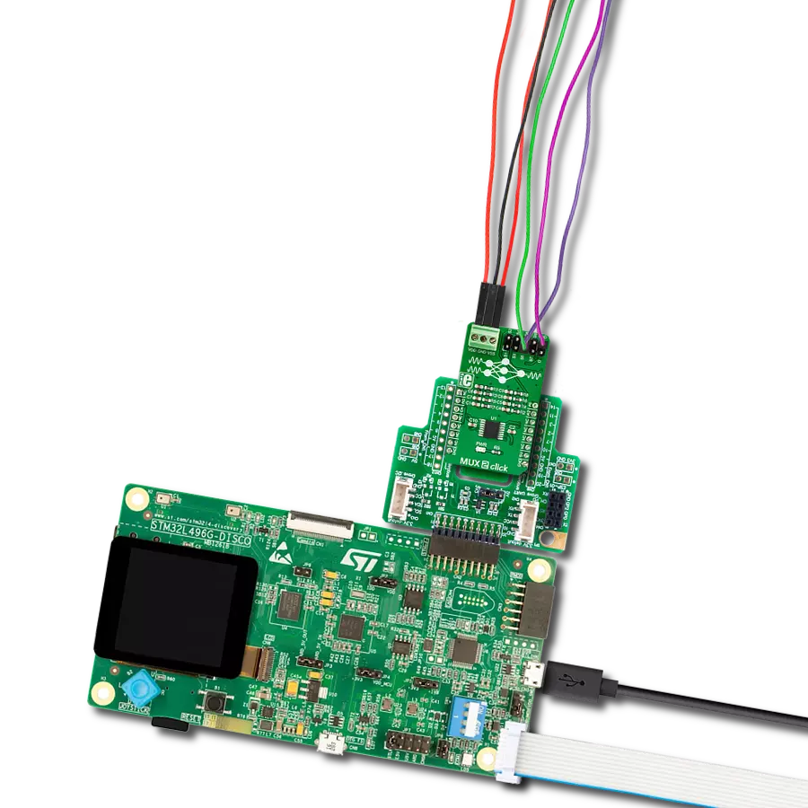
Dev. board
Clicker 2 for Kinetis
Compiler
NECTO Studio
MCU
MK64FN1M0VDC12
Designed for precision, it transforms digital insights into analog realities, enabling seamless communication and decision-making
A
A
Hardware Overview
How does it work?
DAC 4 Click is based on the MCP4728, a quad, 12-bit voltage output Digital-to-Analog converter (DAC) with nonvolatile memory (EEPROM) from Microchip. Its onboard precision output amplifier allows it to achieve rail-to-rail analog output swing. The DAC input codes, device configuration bits, and I2C address bits are programmable to the nonvolatile memory (EEPROM) using I2C serial interface commands. The nonvolatile memory feature enables the DAC device to hold the DAC input codes during power-off time, allowing the DAC outputs to be available immediately after power-up with the saved settings. The MCP4728 device has a high-precision internal voltage reference (VREF = 2.048V). The user can select the internal reference, or an external reference may be used (VDD) for each channel individually. This
gives the ADC 4-click good flexibility for use in various applications. Each channel can be operated individually in Normal mode or Power-Down mode by setting the configuration register bits. In Power-Down mode, most of the internal circuits in the powered-down channel are turned off for power savings, and the output amplifier can be configured to present a known low, medium, or high resistance output load. This device also includes a Power-on Reset (POR) circuit to ensure reliable power-up and an onboard charge pump for the EEPROM programming voltage. The MCP4728 has four output pins routed to the output terminal blocks (TB1 and TB2). The output range of the DAC is 0 V to VREF or 0 V to 2×V REF. The communication with the main MCU is established over a two-wire I2C compatible serial
interface, with standard (100 kHz), fast (400 kHz), or high speed (3.4 MHz) modes supported. The I2C lines (SCL and SDA) are routed to the dedicated mikroBUS™pins. The LDA pin is a multipurpose GPIO: It can be used as Synchronization input or for the device I2C address selection. RDY pin can also optionally be used to monitor the status of EEPROM programming activity. This Click board™ can operate with either 3.3V or 5V logic voltage levels selected via the VCC SEL jumper. This way, both 3.3V and 5V capable MCUs can use the communication lines properly. Also, this Click board™ comes equipped with a library containing easy-to-use functions and an example code that can be used, as a reference, for further development.


Features overview
Development board
Clicker 2 for Kinetis is a compact starter development board that brings the flexibility of add-on Click boards™ to your favorite microcontroller, making it a perfect starter kit for implementing your ideas. It comes with an onboard 32-bit ARM Cortex-M4F microcontroller, the MK64FN1M0VDC12 from NXP Semiconductors, two mikroBUS™ sockets for Click board™ connectivity, a USB connector, LED indicators, buttons, a JTAG programmer connector, and two 26-pin headers for interfacing with external electronics. Its compact design with clear and easily recognizable silkscreen markings allows you to build gadgets with unique functionalities and
features quickly. Each part of the Clicker 2 for Kinetis development kit contains the components necessary for the most efficient operation of the same board. In addition to the possibility of choosing the Clicker 2 for Kinetis programming method, using a USB HID mikroBootloader or an external mikroProg connector for Kinetis programmer, the Clicker 2 board also includes a clean and regulated power supply module for the development kit. It provides two ways of board-powering; through the USB Micro-B cable, where onboard voltage regulators provide the appropriate voltage levels to each component on the board, or
using a Li-Polymer battery via an onboard battery connector. All communication methods that mikroBUS™ itself supports are on this board, including the well-established mikroBUS™ socket, reset button, and several user-configurable buttons and LED indicators. Clicker 2 for Kinetis is an integral part of the Mikroe ecosystem, allowing you to create a new application in minutes. Natively supported by Mikroe software tools, it covers many aspects of prototyping thanks to a considerable number of different Click boards™ (over a thousand boards), the number of which is growing every day.

Microcontroller Overview
MCU Card / MCU

Architecture
ARM Cortex-M4
MCU Memory (KB)
1024
Silicon Vendor
NXP
Pin count
121
RAM (Bytes)
262144
Used MCU Pins
mikroBUS™ mapper
Take a closer look
Click board™ Schematic

Step by step
Project assembly

Start by selecting your development board and Click board™. Begin with the Clicker 2 for Kinetis as your development board.


Track your results in real time
Application Output
1. Application Output - In Debug mode, the 'Application Output' window enables real-time data monitoring, offering direct insight into execution results. Ensure proper data display by configuring the environment correctly using the provided tutorial.

2. UART Terminal - Use the UART Terminal to monitor data transmission via a USB to UART converter, allowing direct communication between the Click board™ and your development system. Configure the baud rate and other serial settings according to your project's requirements to ensure proper functionality. For step-by-step setup instructions, refer to the provided tutorial.

3. Plot Output - The Plot feature offers a powerful way to visualize real-time sensor data, enabling trend analysis, debugging, and comparison of multiple data points. To set it up correctly, follow the provided tutorial, which includes a step-by-step example of using the Plot feature to display Click board™ readings. To use the Plot feature in your code, use the function: plot(*insert_graph_name*, variable_name);. This is a general format, and it is up to the user to replace 'insert_graph_name' with the actual graph name and 'variable_name' with the parameter to be displayed.

Software Support
Library Description
This library contains API for DAC 4 Click driver.
Key functions:
dac4_voltage_reference_set- Setting channel voltage reference valuesdac4_gain_set- Writing channel gain valuesdac4_data_report- Reading channel data and forming reports
Open Source
Code example
The complete application code and a ready-to-use project are available through the NECTO Studio Package Manager for direct installation in the NECTO Studio. The application code can also be found on the MIKROE GitHub account.
/*!
 * \file
 * \brief Dac4 Click example
 *
 * # Description
 * This application enables usage of digital to analog converter.
 *
 * The demo application is composed of two sections :
 *
 * ## Application Init
 * Initializes I2C driver, executes general call reset and wake up commands.
 *
 * ## Application Task
 * Changes the output voltage of channels every 3 seconds, and displays
 * the channels status on the USB UART.
 *
 * \author MikroE Team
 *
 */
// ------------------------------------------------------------------- INCLUDES

#include "board.h"
#include "log.h"
#include "dac4.h"

// ------------------------------------------------------------------ VARIABLES

static dac4_t dac4;
static log_t logger;

// ------------------------------------------------------- ADDITIONAL FUNCTIONS

void dac4_log_report ( uint8_t channel_no )
{
    dac4_channel_setting_t dac4_channel_buffer[ 8 ];

    dac4_data_report ( &dac4, dac4_channel_buffer );
    channel_no *= 2;

    log_printf( &logger, "--- Power ON bit: " );
    switch ( dac4_channel_buffer[ channel_no ].por_bit )
    {
        case 0:
        {
            log_printf( &logger,"Power OFF\r\n" );
            break;
        }
        case 1:
        {
            log_printf( &logger, "Power ON\r\n" );
            break;
        }
        default :
        {
            break;
        }
    }

    log_printf( &logger, "--- V reference    : " );
    switch ( dac4_channel_buffer[ channel_no ].voltage_reference )
    {
        case DAC4_VREF_EXTERNAL:
        {
            log_printf( &logger, "External\r\n" );
            break;
        }
        case DAC4_VREF_INTERNAL:
        {
            log_printf( &logger, "Internal\r\n" );
            break;
        }
        default :
        {
            break;
        }
    }

    log_printf( &logger, "--- Power mode     : " );
    switch ( dac4_channel_buffer[ channel_no ].power_mode )
    {
        case DAC4_MODE_NORMAL:
        {
            log_printf( &logger, "Normal\r\n" );
            break;
        }
        case DAC4_MODE_1kOhm:
        {
            log_printf( &logger, "1 kOhm\r\n" );
            break;
        }
        case DAC4_MODE_100kOhm:
        {
            log_printf( &logger, "100 kOhm\r\n" );
            break;
        }
        case DAC4_MODE_500kOhm:
        {
            log_printf( &logger, "500 kOhm\r\n" );
            break;
        }
        default :
        {
            break;
        }
    }

    log_printf( &logger, "--- Gain value     : " );
    switch ( dac4_channel_buffer[ channel_no ].gain_value )
    {
        case DAC4_MODE_NORMAL:
        {
            log_printf( &logger, "1x Gain\r\n" );
            break;
        }
        case DAC4_MODE_1kOhm:
        {
            log_printf( &logger, "2x Gain\r\n" );
            break;
        }
        default :
        {
            break;
        }
    }

    log_printf( &logger, "--- DAC input data : %d  [0-4095]\r\n", dac4_channel_buffer[ channel_no ].dac_input_data );
    log_printf( &logger, "-------------------------------------\r\n" );
}

void dac4_set_output ( uint8_t channel_set )
{
    dac4_channel_setting_t dac4_channel_x;
    static uint16_t aux_dac_input_data = 0;

    dac4_channel_x.channel_select = channel_set;
    dac4_channel_x.udac_bit = DAC4_UPDATE;
    dac4_channel_x.voltage_reference = DAC4_VREF_EXTERNAL;
    dac4_channel_x.power_mode = DAC4_MODE_NORMAL;
    dac4_channel_x.gain_value = DAC4_GAIN_x1;
    dac4_channel_x.dac_input_data = aux_dac_input_data;

    if ( 0 != dac4_single_write( &dac4, &dac4_channel_x ) )
    {
        log_printf( &logger, "--- Fatal ERROR !!! \r\n" );
    }
    else
    {
        log_printf( &logger, "------------------------------------- \r\n" );
        log_printf( &logger, "--- Output setup done \r\n" );
        log_printf( &logger, "------------------------------------- \r\n" );
        aux_dac_input_data += 500;
        if ( aux_dac_input_data > 4095 )
        {
            aux_dac_input_data = 0;
        }
    }
}

void dac4_channel_report ( )
{
    log_printf( &logger, "\r\n -----> Channel A \r\n" );
    dac4_set_output( DAC4_CHANNEL_A );
    dac4_log_report( 0 );
    Delay_ms ( 1000 );
    Delay_ms ( 1000 );
    Delay_ms ( 1000 );

    log_printf( &logger, "\r\n -----> Channel B \r\n" );
    dac4_set_output( DAC4_CHANNEL_B );
    dac4_log_report( 1 );
    Delay_ms ( 1000 );
    Delay_ms ( 1000 );
    Delay_ms ( 1000 );

    log_printf( &logger, "\r\n -----> Channel C \r\n" );
    dac4_set_output( DAC4_CHANNEL_C );
    dac4_log_report( 2 );
    Delay_ms ( 1000 );
    Delay_ms ( 1000 );
    Delay_ms ( 1000 );

    log_printf( &logger, "\r\n -----> Channel D \r\n" );
    dac4_set_output( DAC4_CHANNEL_D );
    dac4_log_report( 3 );
    Delay_ms ( 1000 );
    Delay_ms ( 1000 );
    Delay_ms ( 1000 );
}

// ------------------------------------------------------ APPLICATION FUNCTIONS

void application_init ( void )
{
    log_cfg_t log_cfg;
    dac4_cfg_t cfg;

    /**
     * Logger initialization.
     * Default baud rate: 115200
     * Default log level: LOG_LEVEL_DEBUG
     * @note If USB_UART_RX and USB_UART_TX
     * are defined as HAL_PIN_NC, you will
     * need to define them manually for log to work.
     * See @b LOG_MAP_USB_UART macro definition for detailed explanation.
     */
    LOG_MAP_USB_UART( log_cfg );
    log_init( &logger, &log_cfg );
    log_info( &logger, "---- Application Init ----" );

    //  Click initialization.

    dac4_cfg_setup( &cfg );
    DAC4_MAP_MIKROBUS( cfg, MIKROBUS_1 );
    dac4_init( &dac4, &cfg );
    log_info( &logger, "---- Application ----" );

    Delay_ms ( 500 );
    dac4_general_call_reset( &dac4 );
    Delay_ms ( 500 );
    dac4_general_call_wake_up( &dac4 );
    Delay_ms ( 500 );

    log_printf( &logger, "--- App init done \r\n \r\n" );
}

void application_task ( void )
{
    dac4_channel_report( );
}

int main ( void )
{
    /* Do not remove this line or clock might not be set correctly. */
    #ifdef PREINIT_SUPPORTED
    preinit();
    #endif

    application_init( );

    for ( ; ; )
    {
        application_task( );
    }

    return 0;
}

// ------------------------------------------------------------------------ END