Convert digital signals into precise analog voltage outputs using the DAC7558 and STM32F407VGT6
12-bit octal-channel voltage-output digital-to-analog (DAC)

Published May 23, 2024
Click board™
DAC 17 Click
Dev. board
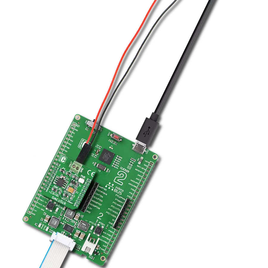
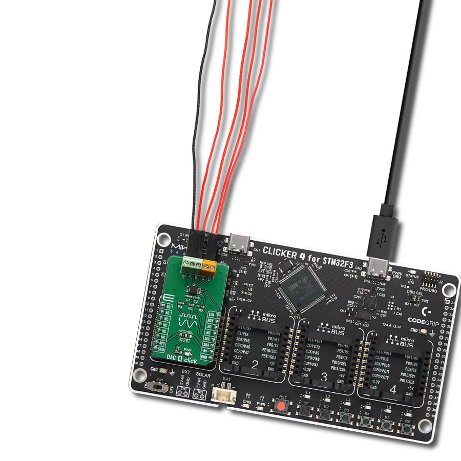
Clicker 4 for STM32F4
Compiler
NECTO Studio
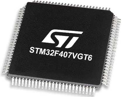
MCU
STM32F407VGT6
Precise voltage output control for applications like digital gain adjustment, programmable voltage sources, and industrial process control.
A
A
Hardware Overview
How does it work?
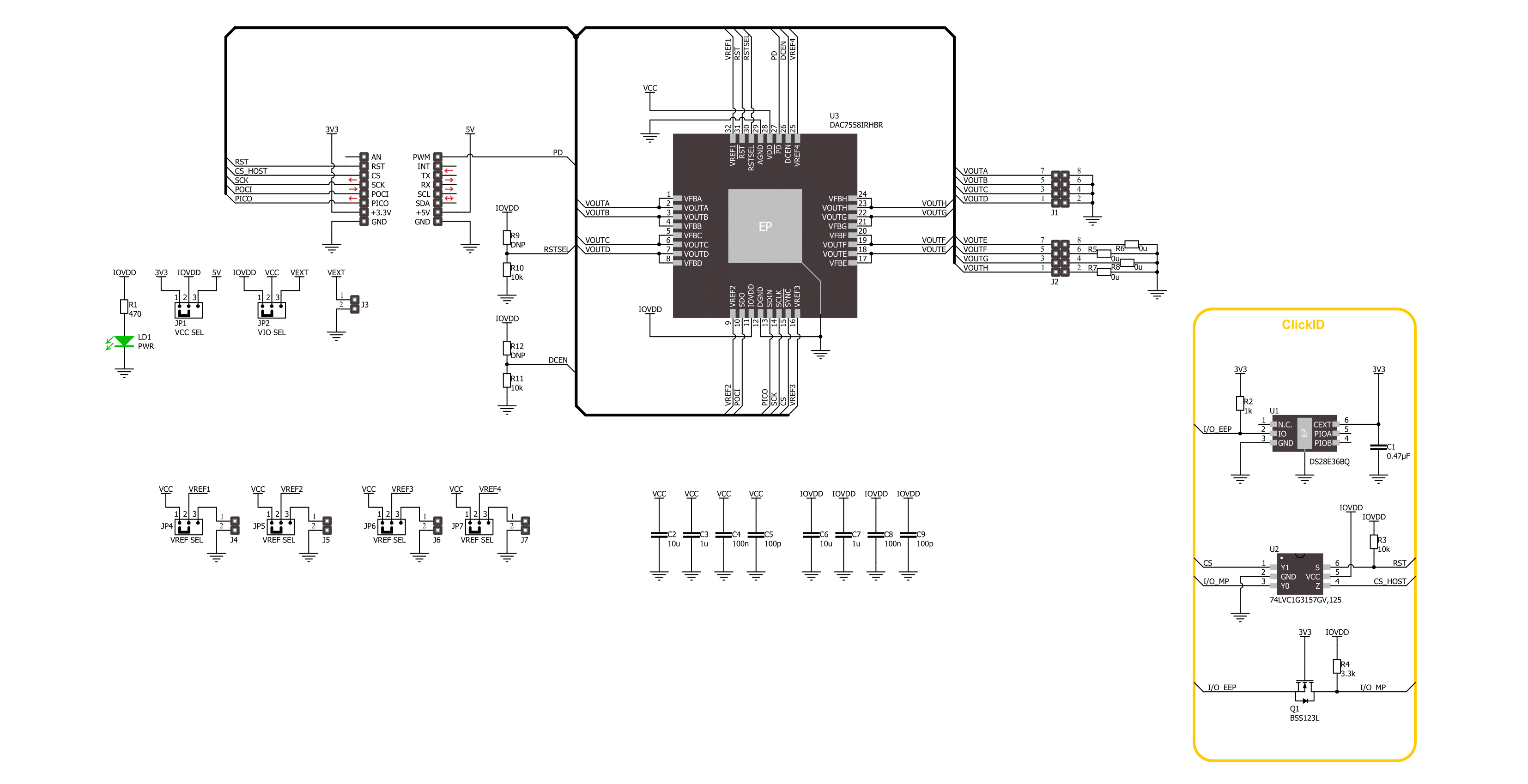
DAC 17 Click is based on the DAC7558, a 12-bit, octal-channel voltage output DAC from Texas Instruments, known for its exceptional linearity and monotonicity. Its proprietary architecture mitigates undesired transients, such as code-to-code glitches and channel-to-channel crosstalk. Operating within a voltage range of 2.7V to 5.5V, the DAC7558 offers versatility. The board provides the flexibility of powering the IC internally or externally by setting the VCC SEL jumper to either the VIO or VEXT position. The VIO option enables internal powering of the Click board™, providing a choice between 3.3V or 5V. On the other hand, the VEXT option allows users to externally supply power in the range of 2.7 to 5.5V (applied to VEXT pins), offering flexibility in power supply according to specific system requirements. Featuring output amplifiers capable of driving a 2Ω, 200pF load rail-to-rail with a rapid settling time of 5µs, the
DAC7558 ensures precise and efficient performance. Users can configure the output range of DAC channels (from CHA to CHH) by connecting an external voltage reference to one of the REFx terminals in a range from 0V to a value of the main IC supply, VCC. Additionally, the board offers a selection between internal and external voltage reference sources. This selection is made via the VREF SEL jumpers, allowing users to choose between internal or external voltage reference options. The DAC7558 offers versatility in operation, with the ability to update outputs simultaneously or sequentially. Its integrated Power-on-Reset circuit guarantees that DAC outputs power up to zero volts during initialization. Furthermore, a Power-Down feature, controllable via the PD pin of the mikroBUS™ socket, reduces the device's current consumption to under 2µA, enhancing efficiency and prolonging battery life.
Communication with the host MCU is achieved through the 4-wire SPI serial interface, supporting clock rates of up to 50MHz. This interface is compatible with SPI, QSPI, Microwire™, and DSP standards, ensuring easy integration into various systems. The DAC7558 also uses an active-low reset feature via the RST pin on the mikroBUS™ socket. When the RST pin is set to a LOW logic state, all DAC channels are reset to zero scale. This Click board™ can operate with either 3.3V or 5V logic voltage levels selected via the VIO SEL jumper. This way, both 3.3V and 5V capable MCUs can use the communication lines properly. Also, this Click board™ comes equipped with a library containing easy-to-use functions and an example code that can be used as a reference for further development.

Features overview
Development board
Clicker 4 for STM32F4 is a compact development board designed as a complete solution that you can use to quickly build your own gadgets with unique functionalities. Featuring an STM32F407VGT6 MCU, four mikroBUS™ sockets for Click boards™ connectivity, power management, and more, it represents a perfect solution for the rapid development of many different types of applications. At its core is an STM32F407VGT6 MCU, a powerful microcontroller by STMicroelectronics based on the high-performance
Arm® Cortex®-M4 32-bit processor core operating at up to 168 MHz frequency. It provides sufficient processing power for the most demanding tasks, allowing Clicker 4 to adapt to any specific application requirements. Besides two 1x20 pin headers, four improved mikroBUS™ sockets represent the most distinctive connectivity feature, allowing access to a huge base of Click boards™, growing on a daily basis. Each section of Clicker 4 is clearly marked, offering an intuitive and clean interface. This makes working with the
development board much simpler and, thus, faster. The usability of Clicker 4 doesn’t end with its ability to accelerate the prototyping and application development stages: it is designed as a complete solution that can be implemented directly into any project, with no additional hardware modifications required. Four mounting holes [4.2mm/0.165”] at all four corners allow simple installation by using mounting screws.

Microcontroller Overview
MCU Card / MCU
Architecture
ARM Cortex-M4
MCU Memory (KB)
10
Silicon Vendor
STMicroelectronics
Pin count
100
RAM (Bytes)
100
Used MCU Pins
mikroBUS™ mapper
Take a closer look
Click board™ Schematic
Step by step
Project assembly

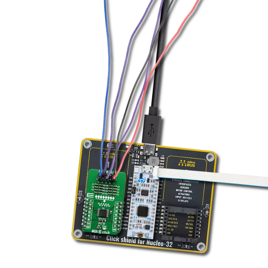
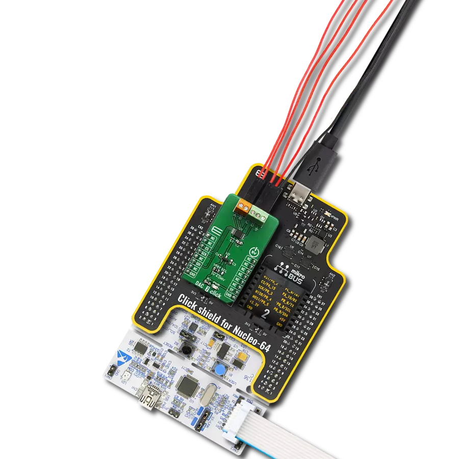
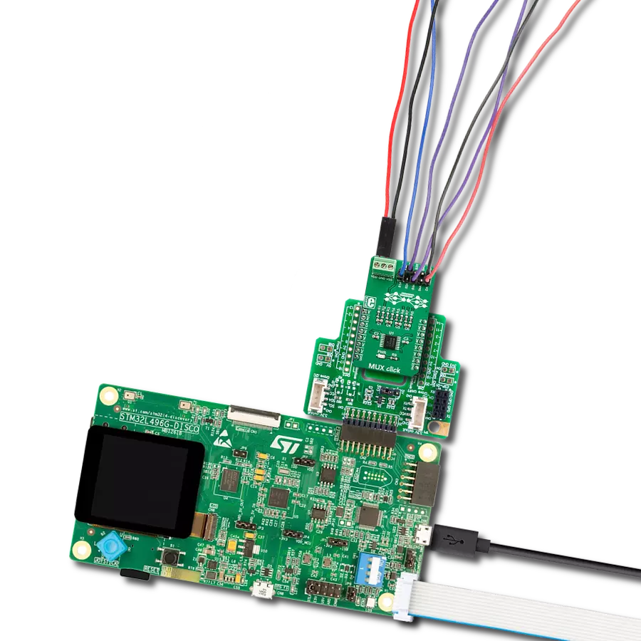
Start by selecting your development board and Click board™. Begin with the Clicker 4 for STM32F4 as your development board.


Software Support
Library Description
This library contains API for DAC 17Click driver.
Key functions:
dac17_send_command- This function is used to send specific command of the DAC 17 click board.dac17_set_dac_output- This function is used to set output level of the sellected channel of the DAC 17 click board.dac17_set_all_dac_output- This function is used to set output level of the DAC 17 click board.
Open Source
Code example
The complete application code and a ready-to-use project are available through the NECTO Studio Package Manager for direct installation in the NECTO Studio. The application code can also be found on the MIKROE GitHub account.
/*!
 * @file main.c
 * @brief DAC 17 Click example
 *
 * # Description
 * This example demonstrates the use of DAC 17 Click board
 * by changing the voltage level on the output channels.
 *
 * The demo application is composed of two sections :
 *
 * ## Application Init
 * Initializes the driver and performs Click default configuration.
 *
 * ## Application Task
 * Changes the output channels voltage level starting from full scale ( REF voltage ),
 * to the mid-scale ( half of the REF voltage ), and then to zero every two seconds.
 *
 * @author Stefan Ilic
 *
 */

#include "board.h"
#include "log.h"
#include "dac17.h"

static dac17_t dac17;
static log_t logger;

void application_init ( void )
{
    log_cfg_t log_cfg;  /**< Logger config object. */
    dac17_cfg_t dac17_cfg;  /**< Click config object. */

    /**
     * Logger initialization.
     * Default baud rate: 115200
     * Default log level: LOG_LEVEL_DEBUG
     * @note If USB_UART_RX and USB_UART_TX
     * are defined as HAL_PIN_NC, you will
     * need to define them manually for log to work.
     * See @b LOG_MAP_USB_UART macro definition for detailed explanation.
     */
    LOG_MAP_USB_UART( log_cfg );
    log_init( &logger, &log_cfg );
    log_info( &logger, " Application Init " );

    // Click initialization.
    dac17_cfg_setup( &dac17_cfg );
    DAC17_MAP_MIKROBUS( dac17_cfg, MIKROBUS_1 );
    if ( SPI_MASTER_ERROR == dac17_init( &dac17, &dac17_cfg ) )
    {
        log_error( &logger, " Communication init." );
        for ( ; ; );
    }

    if ( DAC17_ERROR == dac17_default_cfg ( &dac17 ) )
    {
        log_error( &logger, " Default configuration." );
        for ( ; ; );
    }

    log_info( &logger, " Application Task " );
}

void application_task ( void )
{
    #define DAC17_OUTPUT_ZERO           0x0000u
    #define DAC17_OUTPUT_MID_SCALE      0x0800u
    #define DAC17_OUTPUT_FULL_SCALE     0x0FFFu

    log_printf( &logger, " Setting all channels to full scale output \r\n" );
    dac17_set_all_dac_output( &dac17, DAC17_OUTPUT_FULL_SCALE );
    Delay_ms ( 1000 );
    Delay_ms ( 1000 );

    log_printf( &logger, " Setting all channels outputs to zero \r\n" );
    dac17_set_all_dac_output( &dac17, DAC17_OUTPUT_ZERO );
    Delay_ms ( 1000 );
    Delay_ms ( 1000 );

    log_printf( &logger, " Setting all channels outputs to mid scale \r\n" );
    dac17_set_all_dac_output( &dac17, DAC17_OUTPUT_MID_SCALE );
    Delay_ms ( 1000 );
    Delay_ms ( 1000 );
}

int main ( void )
{
    /* Do not remove this line or clock might not be set correctly. */
    #ifdef PREINIT_SUPPORTED
    preinit();
    #endif

    application_init( );

    for ( ; ; )
    {
        application_task( );
    }

    return 0;
}

// ------------------------------------------------------------------------ END
Additional Support
Resources
Category:DAC