Convert digital data into analog voltages or PWM (triangle or sawtooth) signals with DAC539G2-Q1 and PIC18F57Q43
Smart DAC for general-purpose input to PWM/voltage conversion
Published Sep 26, 2024
Click board™
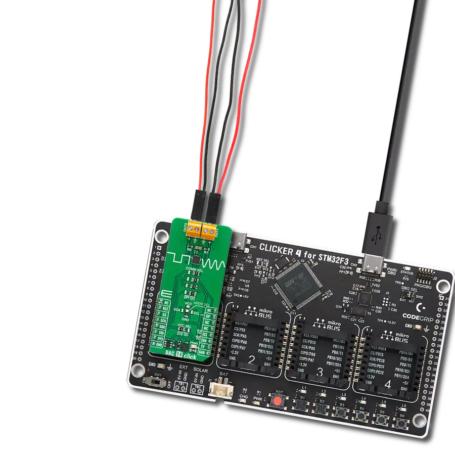
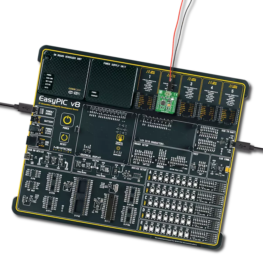
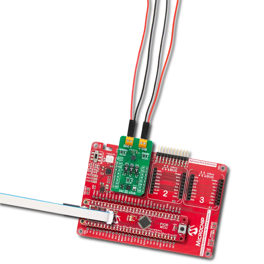
DAC 18 Click
Dev. board
Curiosity Nano with PIC18F57Q43
Compiler
NECTO Studio
MCU
PIC18F57Q43
Excellent choice for fault communication in automotive stop and turn lights and similar industrial applications
A
A
Hardware Overview
How does it work?
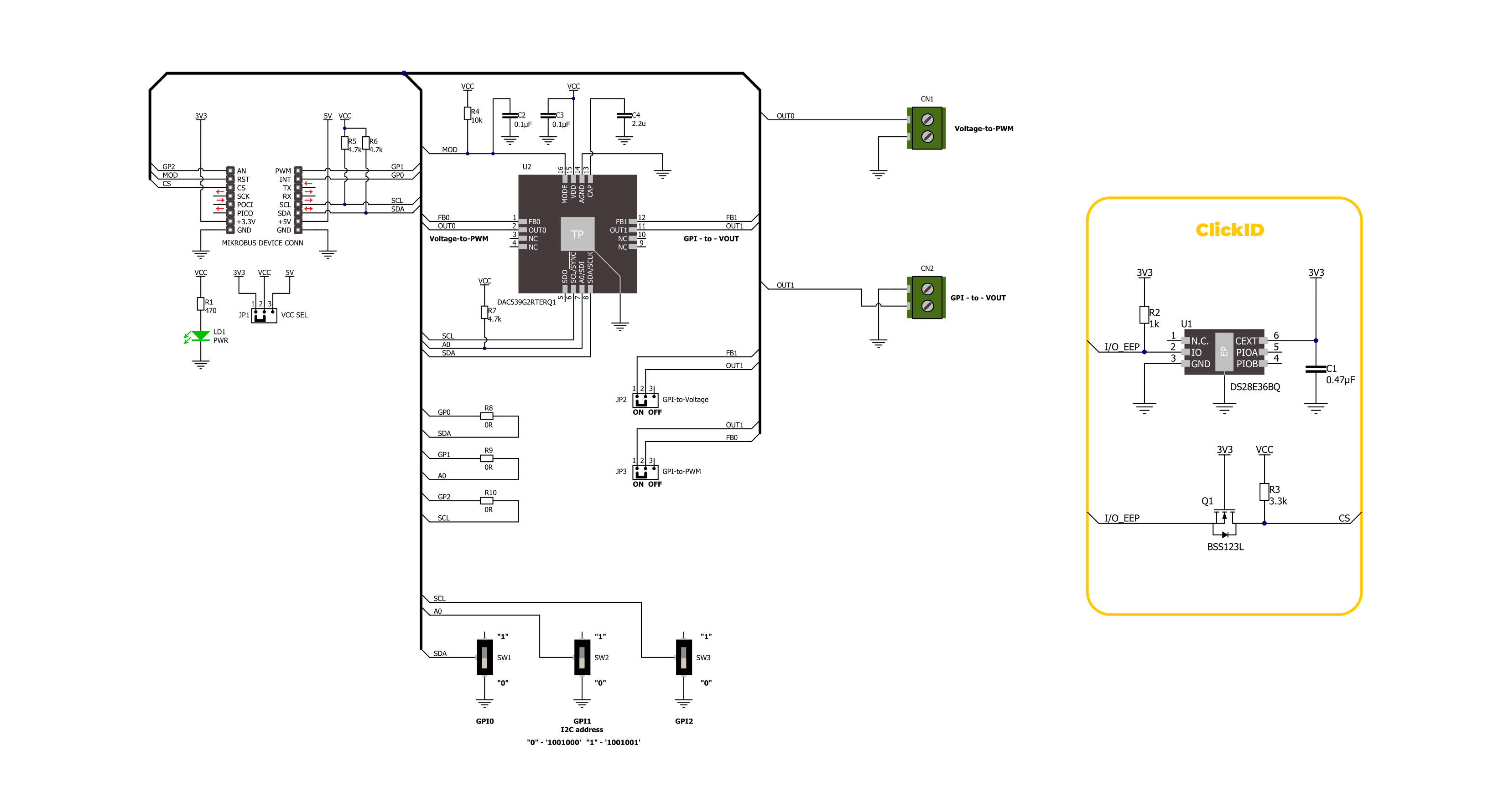
DAC 18 Click is based on the DAC539G2-Q1, a 10-bit smart DAC from Texas Instruments, designed for general-purpose input to PWM conversion. This AEC-Q100-qualified IC functions as a GPI-to-voltage output converter and a voltage-to-PWM converter, generating either sawtooth or triangular waveforms, making it suitable for precise signal generation in various applications. The board uses the operational mode selection pin (MOD) to switch between two operational modes: programming mode, which employs an I2C interface (supporting clock frequencies up to 1MHz), and a standalone mode for autonomous operation without an MCU. What sets DAC 18 Click apart is its nonvolatile memory (NVM) capability, which allows users to store customized register settings during programming via I2C. Once configured, the device can function independently, executing the predefined instructions. This feature makes it ideal
for applications such as fault communication in automotive stop-and-turn lighting systems and broader industrial environments where reliable signal conversion is essential. The DAC539G2-Q1 has a string architecture with two key output channels. Channel 1 operates as a digital-to-analog converter (DAC), providing a voltage output through the OUT1 terminal, while Channel 0 functions as a voltage-to-PWM converter, using either a triangle or sawtooth waveform at the noninverting input of the amplifier, with output available on the OUT0 terminal. Channel 1 also acts as a GPI-to-voltage converter, using a look-up table with eight entries (Table 7-1 in the datasheet), allowing the selection of multiple programmable output voltage ranges based on the binary combinations of three GPI pins, which can be configured via onboard GPx switches. Both functions, PWM and DAC output, can be manually
activated or deactivated using the V-to-PWM and GPI-to-V jumpers by switching them from the ON to the OFF position (by default, both functions are active and provide corresponding output on the OUTx terminals). The three switches can also choose the I2C address in addition to selecting programmable output voltage ranges. Moreover, the general-purpose inputs, aside from manual control, can also be controlled digitally via the GP0-GP2 pins from the mikroBUS™ socket. This Click board™ can operate with either 3.3V or 5V logic voltage levels selected via the VCC SEL jumper. This way, both 3.3V and 5V capable MCUs can use the communication lines properly. Also, this Click board™ comes equipped with a library containing easy-to-use functions and an example code that can be used as a reference for further development.

Features overview
Development board
PIC18F57Q43 Curiosity Nano evaluation kit is a cutting-edge hardware platform designed to evaluate microcontrollers within the PIC18-Q43 family. Central to its design is the inclusion of the powerful PIC18F57Q43 microcontroller (MCU), offering advanced functionalities and robust performance. Key features of this evaluation kit include a yellow user LED and a responsive
mechanical user switch, providing seamless interaction and testing. The provision for a 32.768kHz crystal footprint ensures precision timing capabilities. With an onboard debugger boasting a green power and status LED, programming and debugging become intuitive and efficient. Further enhancing its utility is the Virtual serial port (CDC) and a debug GPIO channel (DGI
GPIO), offering extensive connectivity options. Powered via USB, this kit boasts an adjustable target voltage feature facilitated by the MIC5353 LDO regulator, ensuring stable operation with an output voltage ranging from 1.8V to 5.1V, with a maximum output current of 500mA, subject to ambient temperature and voltage constraints.

Microcontroller Overview
MCU Card / MCU

Architecture
PIC
MCU Memory (KB)
128
Silicon Vendor
Microchip
Pin count
48
RAM (Bytes)
8196
You complete me!
Accessories
Curiosity Nano Base for Click boards is a versatile hardware extension platform created to streamline the integration between Curiosity Nano kits and extension boards, tailored explicitly for the mikroBUS™-standardized Click boards and Xplained Pro extension boards. This innovative base board (shield) offers seamless connectivity and expansion possibilities, simplifying experimentation and development. Key features include USB power compatibility from the Curiosity Nano kit, alongside an alternative external power input option for enhanced flexibility. The onboard Li-Ion/LiPo charger and management circuit ensure smooth operation for battery-powered applications, simplifying usage and management. Moreover, the base incorporates a fixed 3.3V PSU dedicated to target and mikroBUS™ power rails, alongside a fixed 5.0V boost converter catering to 5V power rails of mikroBUS™ sockets, providing stable power delivery for various connected devices.

Used MCU Pins
mikroBUS™ mapper
Take a closer look
Click board™ Schematic
Step by step
Project assembly

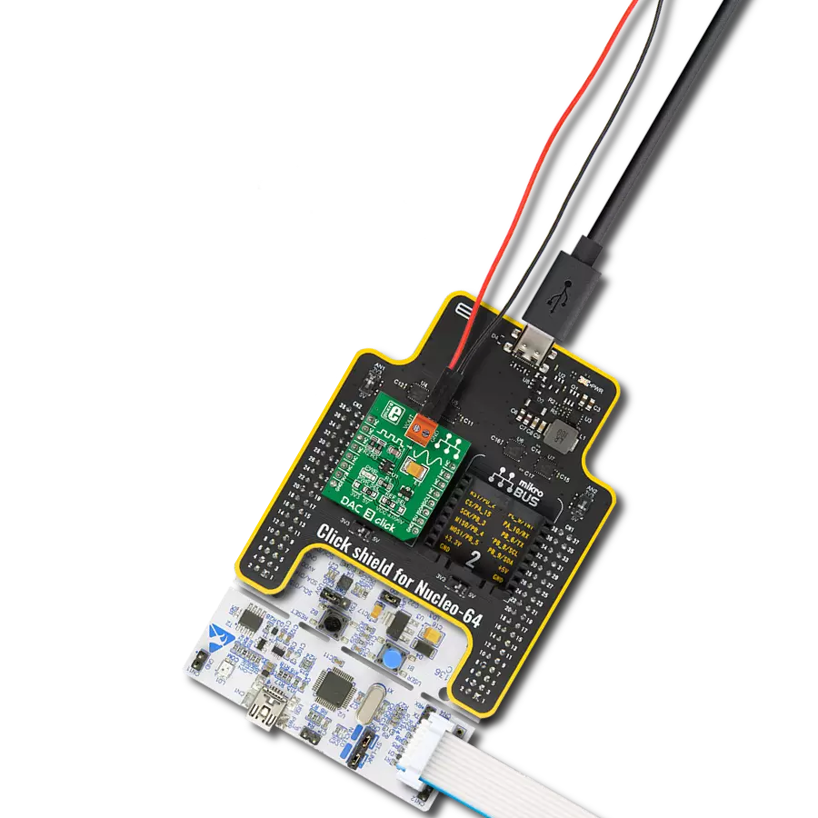
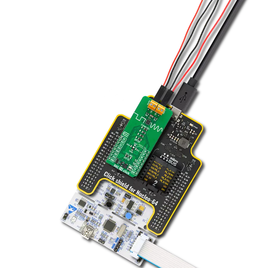
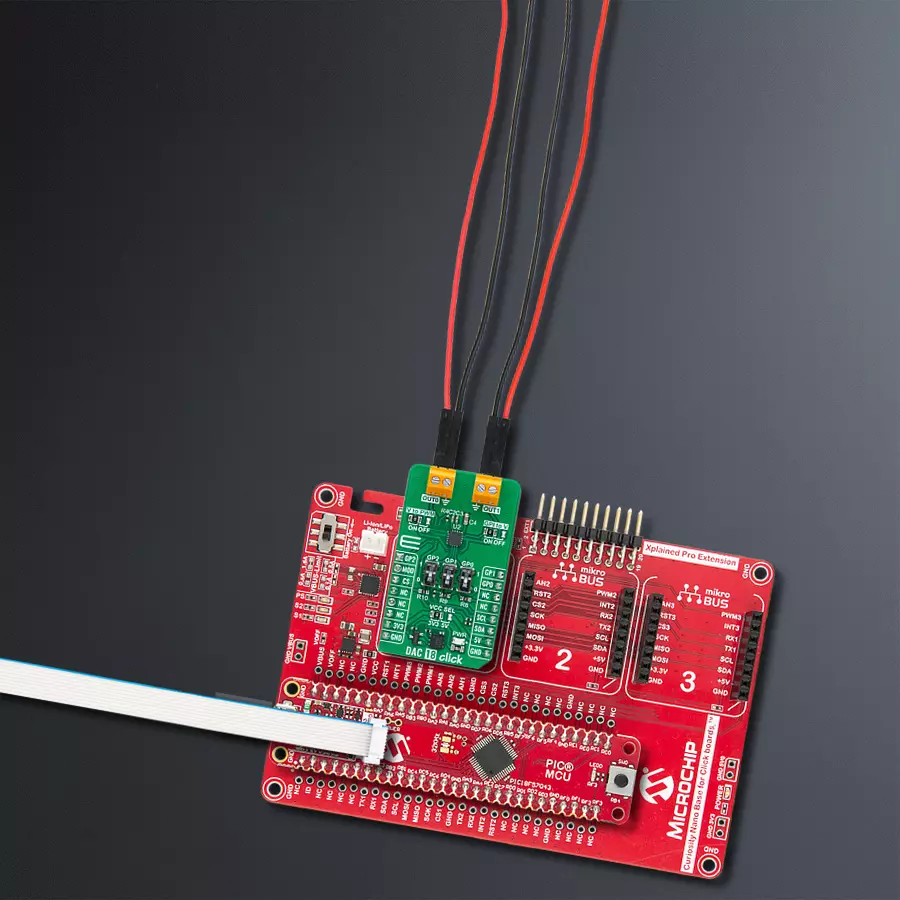
Start by selecting your development board and Click board™. Begin with the Curiosity Nano with PIC18F57Q43 as your development board.


Track your results in real time
Application Output
1. Application Output - In Debug mode, the 'Application Output' window enables real-time data monitoring, offering direct insight into execution results. Ensure proper data display by configuring the environment correctly using the provided tutorial.

2. UART Terminal - Use the UART Terminal to monitor data transmission via a USB to UART converter, allowing direct communication between the Click board™ and your development system. Configure the baud rate and other serial settings according to your project's requirements to ensure proper functionality. For step-by-step setup instructions, refer to the provided tutorial.

3. Plot Output - The Plot feature offers a powerful way to visualize real-time sensor data, enabling trend analysis, debugging, and comparison of multiple data points. To set it up correctly, follow the provided tutorial, which includes a step-by-step example of using the Plot feature to display Click board™ readings. To use the Plot feature in your code, use the function: plot(*insert_graph_name*, variable_name);. This is a general format, and it is up to the user to replace 'insert_graph_name' with the actual graph name and 'variable_name' with the parameter to be displayed.

Software Support
Library Description
This library contains API for DAC 18 Click driver.
Key functions:
dac18_cfg_pwm_out- This function configures PWM output (OUT0) for the function generator by using the I2C serial interface.dac18_set_mode- This function selects between programming and standalone modes by toggling the digital output state of the MOD pin.dac18_get_gpi_status- This function gets GPI status by reading the states of the GP0, GP1 and GP2 pins.
Open Source
Code example
The complete application code and a ready-to-use project are available through the NECTO Studio Package Manager for direct installation in the NECTO Studio. The application code can also be found on the MIKROE GitHub account.
/*!
 * @file main.c
 * @brief DAC 18 Click example
 *
 * # Description
 * This example demonstrates the use of the DAC 18 Click board
 * by configuring the waveform signals from a function generator on the OUT0
 * and voltage level on the OUT1.
 *
 * The demo application is composed of two sections :
 *
 * ## Application Init
 * Initialization of I2C module and log UART.
 * After driver initialization, the app executes a default configuration (configuration mode).
 *
 * ## Application Task
 * The demo application operated in standalone mode and displayed the voltage level on OUT1.
 * The GP0, GP1, and GP2 switches on the DAC 18 Click board
 * are used to change the output voltage level and waveform signals.
 * Results are being sent to the UART Terminal, where you can track their changes.
 *
 * ## Additional Function
 * - static void dac18_display_out_status ( uint8_t status )
 *
 * @note
 * Set GP0, GP1, and GP2 switches to position "1" for the configuration modes.
 *
 * @author Nenad Filipovic
 *
 */

#include "board.h"
#include "log.h"
#include "dac18.h"

static dac18_t dac18;
static log_t logger;

static uint8_t gpi_status = 0;
static uint8_t new_gpi_status = 7;

/**
 * @brief DAC 18 display output states.
 * @details This function displays OUT0 and OUT1 status.
 * @note None.
 */
static void dac18_display_out_status ( void );

void application_init ( void )
{
    log_cfg_t log_cfg;  /**< Logger config object. */
    dac18_cfg_t dac18_cfg;  /**< Click config object. */

    /**
     * Logger initialization.
     * Default baud rate: 115200
     * Default log level: LOG_LEVEL_DEBUG
     * @note If USB_UART_RX and USB_UART_TX
     * are defined as HAL_PIN_NC, you will
     * need to define them manually for log to work.
     * See @b LOG_MAP_USB_UART macro definition for detailed explanation.
     */
    LOG_MAP_USB_UART( log_cfg );
    log_init( &logger, &log_cfg );
    log_info( &logger, " Application Init " );

    // Click initialization.
    dac18_cfg_setup( &dac18_cfg );
    DAC18_MAP_MIKROBUS( dac18_cfg, MIKROBUS_1 );
    if ( I2C_MASTER_ERROR == dac18_init( &dac18, &dac18_cfg ) )
    {
        log_error( &logger, " Communication init." );
        for ( ; ; );
    }

    if ( DAC18_ERROR == dac18_default_cfg ( &dac18 ) )
    {
        log_error( &logger, " Default configuration." );
        for ( ; ; );
    }

    log_info( &logger, " Application Task " );
    log_printf( &logger, " Use the GP0, GP1 and GP2 switch to change the outputs\r\n\n" );
}

void application_task ( void )
{
    dac18_get_gpi_status( &dac18, &gpi_status );
    if ( gpi_status != new_gpi_status )
    {
        new_gpi_status = gpi_status;
        dac18_display_out_status( );
    }
    Delay_ms ( 100 );
}

int main ( void )
{
    /* Do not remove this line or clock might not be set correctly. */
    #ifdef PREINIT_SUPPORTED
    preinit();
    #endif

    application_init( );

    for ( ; ; )
    {
        application_task( );
    }

    return 0;
}

static void dac18_display_out_status ( void )
{
    switch ( gpi_status )
    {
        case 0: case 4:
        {
            log_printf( &logger, " OUT0 Duty-cycle: 80 [%%]\r\n" );
            log_printf( &logger, " OUT1 Voltage: 0.75 [V]\r\n\n" );
            break;
        }
        case 1: case 5:
        {
            log_printf( &logger, " OUT0 Duty-cycle: 20 [%%]\r\n" );
            log_printf( &logger, " OUT1 Voltage: 2.00 [V]\r\n\n" );
            break;
        }
        case 2: case 6:
        {
            log_printf( &logger, " OUT0 Duty-cycle: 60 [%%]\r\n" );
            log_printf( &logger, " OUT1 Voltage: 1.16 [V]\r\n\n" );
            break;
        }
        case 3: case 7:
        {
            log_printf( &logger, " OUT0 Duty-cycle: 40 [%%]\r\n" );
            log_printf( &logger, " OUT1 Voltage: 1.58 [V]\r\n\n" );
            break;
        }
        default:
        {
            log_printf( &logger, " Unknown\r\n" );
        }
    }
}

// ------------------------------------------------------------------------ END
Additional Support
Resources
Category:DAC