Preserve user settings and preferences with DS28EC20 and PIC18F57Q43
Future-proofing solutions with EEPROM innovation

Published Feb 13, 2024
Click board™
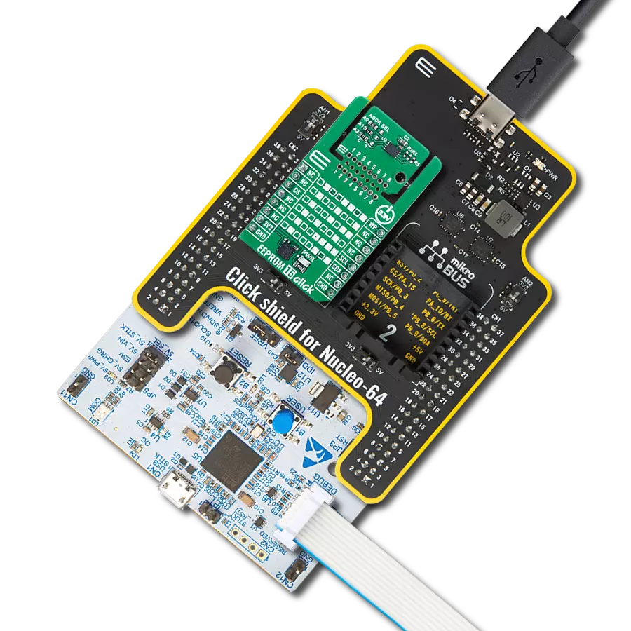
EEPROM 6 Click
Dev. board
Curiosity Nano with PIC18F57Q43
Compiler
NECTO Studio
MCU
PIC18F57Q43
Through the strategic use of EEPROM memory, our solution addresses the challenges of data persistence and management, enabling you to focus on innovation and growth
A
A
Hardware Overview
How does it work?
EEPROM 6 Click is based on the DS28EC20, a 20Kb data EEPROM with a fully featured 1-Wire interface in a single chip from Analog Devices. The memory is organized as 80 pages of 256 bits each. In addition, the device has one page for control functions such as permanent write protection and EPROM-Emulation mode for individual 2048-bit (8-page) memory blocks. A volatile 256-bit memory page called the scratchpad acts as a buffer when writing data to the EEPROM to ensure data integrity. Data is first written to the scratchpad, from which it can be read back for verification before transferring it to the EEPROM. Each DS28EC20 has its own unalterable and unique 64-bit registration number.
The registration number guarantees unique identification and addresses the device in a multidrop 1-Wire net environment. In addition to the EEPROM, the device has a 32-byte volatile scratchpad. Writes to the EEPROM array are a two-step process. First, data is written to the scratchpad and then copied into the main array. The user can verify the data in the scratchpad before copying. The EEPROM 6 Click communicates with MCU using the 1-Wire interface, which supports a Standard and Overdrive communication speed of 15.4kbps (max) and 90kbps (max). If not explicitly set into the Overdrive mode, the DS28EC20 communicates at Standard speed. The 1-Wire communication line is
routed to the SMD jumper labeled GP SEL, which allows routing of the 1-Wire communication either to the PWM pin or the AN pin of the mikroBUS™ socket. These pins are labeled GP0 and GP1, respectively, the same as the SMD jumper positions, making the selection of the desired pin simple and straightforward. This Click board™ can operate with either 3.3V or 5V logic voltage levels selected via the VCC SEL jumper. This way, both 3.3V and 5V capable MCUs can use the communication lines properly. Also, this Click board™ comes equipped with a library containing easy-to-use functions and an example code that can be used, as a reference, for further development.


Features overview
Development board
PIC18F57Q43 Curiosity Nano evaluation kit is a cutting-edge hardware platform designed to evaluate microcontrollers within the PIC18-Q43 family. Central to its design is the inclusion of the powerful PIC18F57Q43 microcontroller (MCU), offering advanced functionalities and robust performance. Key features of this evaluation kit include a yellow user LED and a responsive
mechanical user switch, providing seamless interaction and testing. The provision for a 32.768kHz crystal footprint ensures precision timing capabilities. With an onboard debugger boasting a green power and status LED, programming and debugging become intuitive and efficient. Further enhancing its utility is the Virtual serial port (CDC) and a debug GPIO channel (DGI
GPIO), offering extensive connectivity options. Powered via USB, this kit boasts an adjustable target voltage feature facilitated by the MIC5353 LDO regulator, ensuring stable operation with an output voltage ranging from 1.8V to 5.1V, with a maximum output current of 500mA, subject to ambient temperature and voltage constraints.

Microcontroller Overview
MCU Card / MCU

Architecture
PIC
MCU Memory (KB)
128
Silicon Vendor
Microchip
Pin count
48
RAM (Bytes)
8196
You complete me!
Accessories
Curiosity Nano Base for Click boards is a versatile hardware extension platform created to streamline the integration between Curiosity Nano kits and extension boards, tailored explicitly for the mikroBUS™-standardized Click boards and Xplained Pro extension boards. This innovative base board (shield) offers seamless connectivity and expansion possibilities, simplifying experimentation and development. Key features include USB power compatibility from the Curiosity Nano kit, alongside an alternative external power input option for enhanced flexibility. The onboard Li-Ion/LiPo charger and management circuit ensure smooth operation for battery-powered applications, simplifying usage and management. Moreover, the base incorporates a fixed 3.3V PSU dedicated to target and mikroBUS™ power rails, alongside a fixed 5.0V boost converter catering to 5V power rails of mikroBUS™ sockets, providing stable power delivery for various connected devices.

Used MCU Pins
mikroBUS™ mapper
Take a closer look
Click board™ Schematic

Step by step
Project assembly

Start by selecting your development board and Click board™. Begin with the Curiosity Nano with PIC18F57Q43 as your development board.


Track your results in real time
Application Output
1. Application Output - In Debug mode, the 'Application Output' window enables real-time data monitoring, offering direct insight into execution results. Ensure proper data display by configuring the environment correctly using the provided tutorial.

2. UART Terminal - Use the UART Terminal to monitor data transmission via a USB to UART converter, allowing direct communication between the Click board™ and your development system. Configure the baud rate and other serial settings according to your project's requirements to ensure proper functionality. For step-by-step setup instructions, refer to the provided tutorial.

3. Plot Output - The Plot feature offers a powerful way to visualize real-time sensor data, enabling trend analysis, debugging, and comparison of multiple data points. To set it up correctly, follow the provided tutorial, which includes a step-by-step example of using the Plot feature to display Click board™ readings. To use the Plot feature in your code, use the function: plot(*insert_graph_name*, variable_name);. This is a general format, and it is up to the user to replace 'insert_graph_name' with the actual graph name and 'variable_name' with the parameter to be displayed.

Software Support
Library Description
This library contains API for EEPROM 6 Click driver.
Key functions:
eprom6_write_mem- This function writes a sequential data starting of the targeted 16b register address of the targeted 16-bit register address of the DS28EC20eeprom6_read_mem- This function reads a sequential data starting from the targeted 16-bit register address of the DS28EC20.
Open Source
Code example
The complete application code and a ready-to-use project are available through the NECTO Studio Package Manager for direct installation in the NECTO Studio. The application code can also be found on the MIKROE GitHub account.
/*!
 * @file main.c
 * @brief EEPROM 6 Click Example.
 *
 * # Description
 * This example demonstrates the use of EEPROM6 Click board by writing
 * string to a memory at some specific location and then reading it back.
 *
 * The demo application is composed of two sections :
 *
 * ## Application Init
 * Initializes the driver and performs the Click default configuration.
 *
 * ## Application Task
 * This example shows capabilities of EEPROM 6 Click board by writting a string
 * into memory location from a specific address, and then reading it back every 5 seconds.
 *
 * @author Nikola Citakovic
 *
 */

#include "board.h"
#include "log.h"
#include "eeprom6.h"

static eeprom6_t eeprom6;
static log_t logger;

#define EEPROM6_DEMO_TEXT       "MikroE - EEPROM 6 Click board"
#define EEPROM6_TEXT_ADDRESS    0x0000

void application_init ( void )
{
    log_cfg_t log_cfg;  /**< Logger config object. */
    eeprom6_cfg_t eeprom6_cfg;  /**< Click config object. */

    /**
     * Logger initialization.
     * Default baud rate: 115200
     * Default log level: LOG_LEVEL_DEBUG
     * @note If USB_UART_RX and USB_UART_TX
     * are defined as HAL_PIN_NC, you will
     * need to define them manually for log to work.
     * See @b LOG_MAP_USB_UART macro definition for detailed explanation.
     */
    LOG_MAP_USB_UART( log_cfg );
    log_init( &logger, &log_cfg );
    log_info( &logger, " Application Init " );

    // Click initialization.
    eeprom6_cfg_setup( &eeprom6_cfg );
    EEPROM6_MAP_MIKROBUS( eeprom6_cfg, MIKROBUS_1 );
    if ( ONE_WIRE_ERROR == eeprom6_init( &eeprom6, &eeprom6_cfg ) )
    {
        log_error( &logger, " Communication init." );
        for ( ; ; );
    }

    if ( EEPROM6_ERROR == eeprom6_default_cfg ( &eeprom6 ) )
    {
        log_error( &logger, " Default configuration." );
        for ( ; ; );
    }

    log_info( &logger, " Application Task " );
}

void application_task ( void )
{
    log_printf( &logger, "Writing \"%s\" to memory address 0x%.4X\r\n",
                ( uint8_t * ) EEPROM6_DEMO_TEXT, EEPROM6_TEXT_ADDRESS );
    eeprom6_write_mem( &eeprom6, EEPROM6_TEXT_ADDRESS, ( char * ) EEPROM6_DEMO_TEXT,
                       strlen ( EEPROM6_DEMO_TEXT ) );
    Delay_ms ( 100 );
    uint8_t read_buf[ 100 ] = { 0 };
    eeprom6_read_mem ( &eeprom6, EEPROM6_TEXT_ADDRESS,read_buf,
                       strlen ( EEPROM6_DEMO_TEXT ) );
    log_printf( &logger, "Reading \"%s\" from memory address 0x%.4X\r\n\n",
                read_buf, ( uint16_t ) EEPROM6_TEXT_ADDRESS );
    Delay_ms ( 1000 );
    Delay_ms ( 1000 );
    Delay_ms ( 1000 );
    Delay_ms ( 1000 );
    Delay_ms ( 1000 );
}

int main ( void )
{
    /* Do not remove this line or clock might not be set correctly. */
    #ifdef PREINIT_SUPPORTED
    preinit();
    #endif

    application_init( );

    for ( ; ; )
    {
        application_task( );
    }

    return 0;
}

// ------------------------------------------------------------------------ END
Additional Support
Resources
Category:EEPROM