Increase (boost) a low voltage from a battery or other source to a stable 3.3V output with the XCL105B331H2-G and PIC18F57Q43
Synchronous step-up DC/DC converter with integrated switching FETs

Published Jun 04, 2024
Click board™
Boost 11 Click
Dev. board
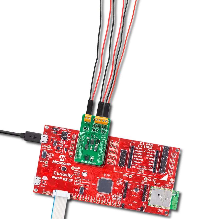
Curiosity Nano with PIC18F57Q43
Compiler
NECTO Studio
MCU
PIC18F57Q43
Provide a reliable voltage boost for powering low-power sensors or other industrial electronics from low-voltage sources
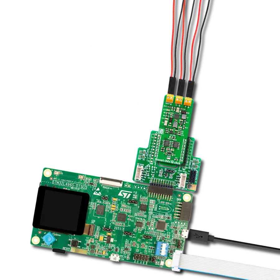
A
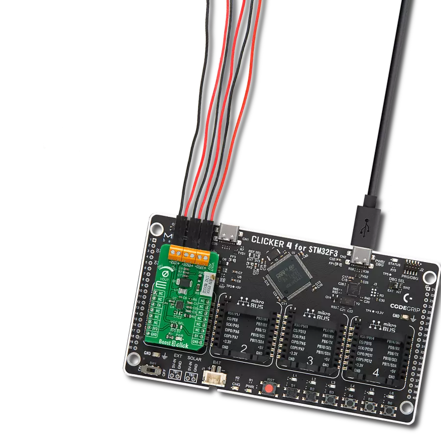
A
Hardware Overview
How does it work?
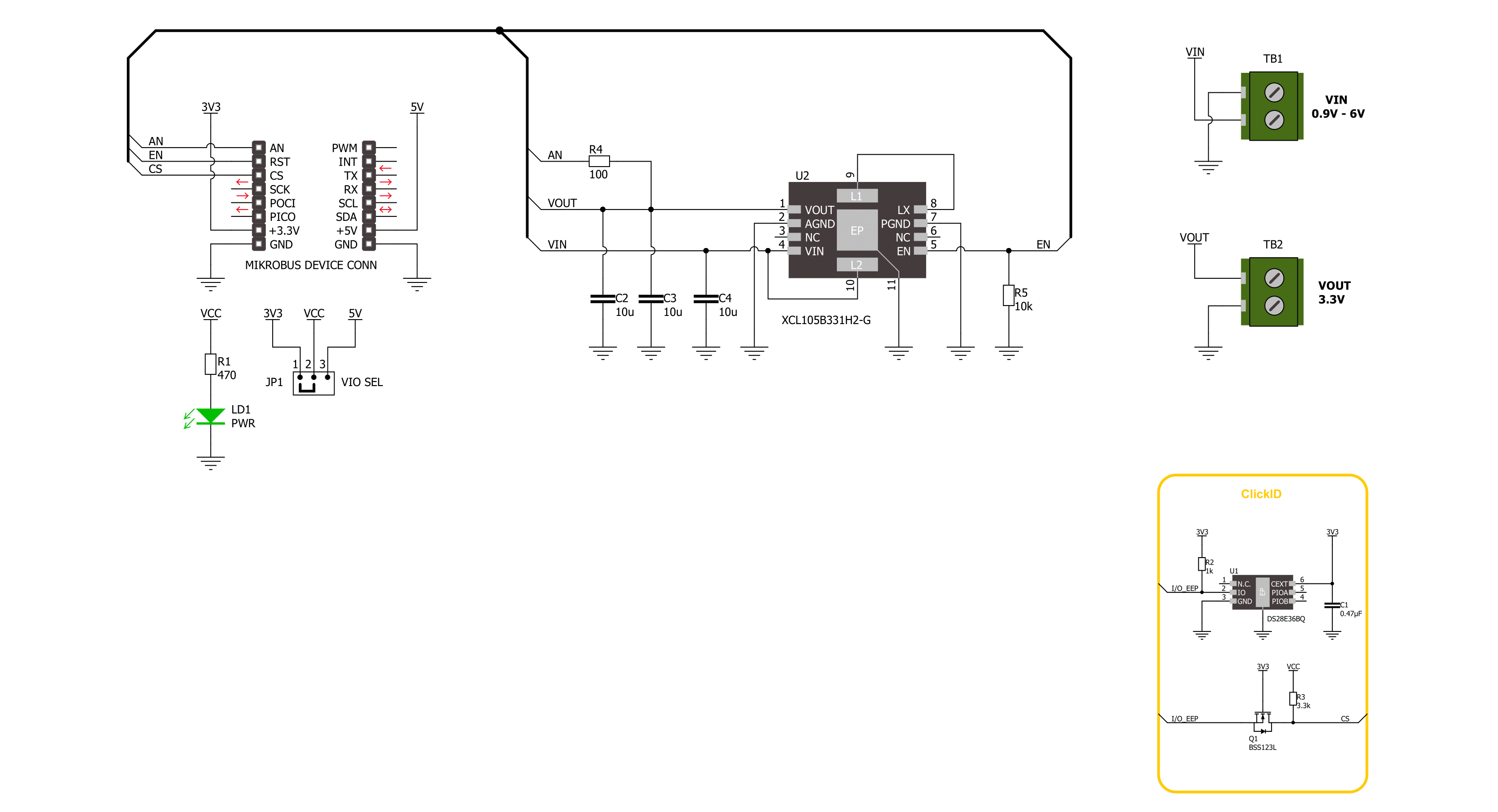
Boost 11 Click is based on the XCL105B331H2-G, a synchronous step-up DC/DC converter from TOREX Semi. This component includes a reference voltage source, ramp wave circuit, error amplifier, PWM comparator, phase compensation circuit, N-channel driver FET, P-channel synchronous switching FET, and current limiter circuit. It can start operating from an input voltage of 0.9V, making it suitable for devices using single Alkaline or Nickel-metal hydride batteries. The operating voltage range spans from 0.9V to 6V, which applies to the VIN terminal. This versatility makes it ideal for industrial equipment, Internet of Things (IoT) devices, wearables, and any applications
prioritizing battery life. The XCL105B331H2-G operates by using the error amplifier to compare the internal reference voltage with the feedback voltage. The resulting output undergoes phase compensation and is fed to the PWM comparator. This comparator matches the signal from the error amplifier with the ramp wave circuit output, sending the resulting signal to the buffer driver circuit to control the PWM duty cycle. This continuous process stabilizes the output voltage, fixed at 3.3V and available at the VOUT terminal. Additionally, an output signal is available on the AN pin of the mikroBUS™ socket. The Boost 11 Click uses the EN pin of the mikroBUS™ socket in addition to the
AN pin. When the EN pin is set to a high logic level, the output voltage is raised via the Start-Up mode, initiating normal operation. When set to a low logic level, the IC enters Standby mode, significantly reducing current consumption. This Click board™ can operate with either 3.3V or 5V logic voltage levels selected via the VIO SEL jumper. This way, both 3.3V and 5V capable MCUs can use the communication lines properly. Also, this Click board™ comes equipped with a library containing easy-to-use functions and an example code that can be used as a reference for further development.

Features overview
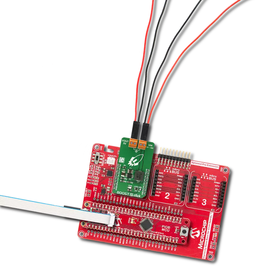
Development board
PIC18F57Q43 Curiosity Nano evaluation kit is a cutting-edge hardware platform designed to evaluate microcontrollers within the PIC18-Q43 family. Central to its design is the inclusion of the powerful PIC18F57Q43 microcontroller (MCU), offering advanced functionalities and robust performance. Key features of this evaluation kit include a yellow user LED and a responsive
mechanical user switch, providing seamless interaction and testing. The provision for a 32.768kHz crystal footprint ensures precision timing capabilities. With an onboard debugger boasting a green power and status LED, programming and debugging become intuitive and efficient. Further enhancing its utility is the Virtual serial port (CDC) and a debug GPIO channel (DGI
GPIO), offering extensive connectivity options. Powered via USB, this kit boasts an adjustable target voltage feature facilitated by the MIC5353 LDO regulator, ensuring stable operation with an output voltage ranging from 1.8V to 5.1V, with a maximum output current of 500mA, subject to ambient temperature and voltage constraints.

Microcontroller Overview
MCU Card / MCU

Architecture
PIC
MCU Memory (KB)
128
Silicon Vendor
Microchip
Pin count
48
RAM (Bytes)
8196
You complete me!
Accessories
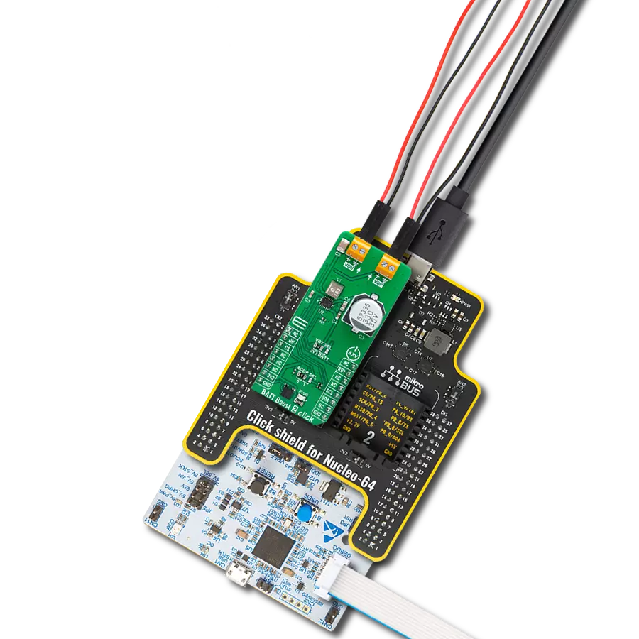
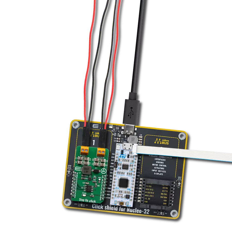
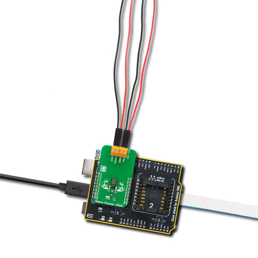
Curiosity Nano Base for Click boards is a versatile hardware extension platform created to streamline the integration between Curiosity Nano kits and extension boards, tailored explicitly for the mikroBUS™-standardized Click boards and Xplained Pro extension boards. This innovative base board (shield) offers seamless connectivity and expansion possibilities, simplifying experimentation and development. Key features include USB power compatibility from the Curiosity Nano kit, alongside an alternative external power input option for enhanced flexibility. The onboard Li-Ion/LiPo charger and management circuit ensure smooth operation for battery-powered applications, simplifying usage and management. Moreover, the base incorporates a fixed 3.3V PSU dedicated to target and mikroBUS™ power rails, alongside a fixed 5.0V boost converter catering to 5V power rails of mikroBUS™ sockets, providing stable power delivery for various connected devices.

Used MCU Pins
mikroBUS™ mapper
Take a closer look
Click board™ Schematic
Step by step
Project assembly

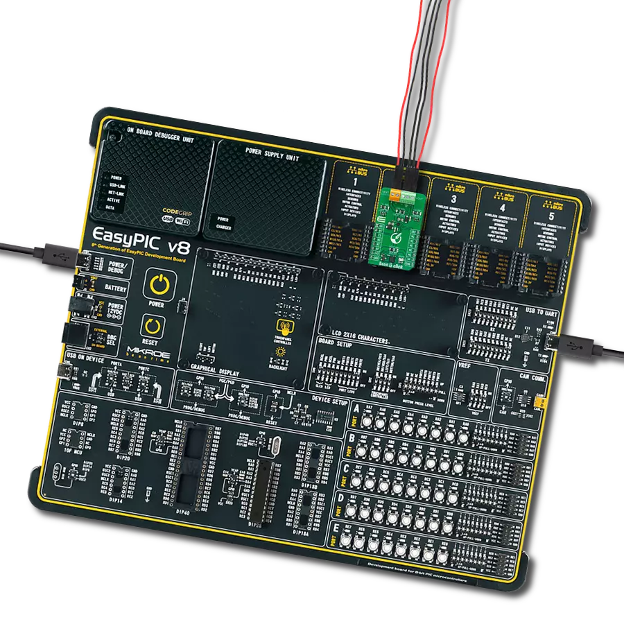
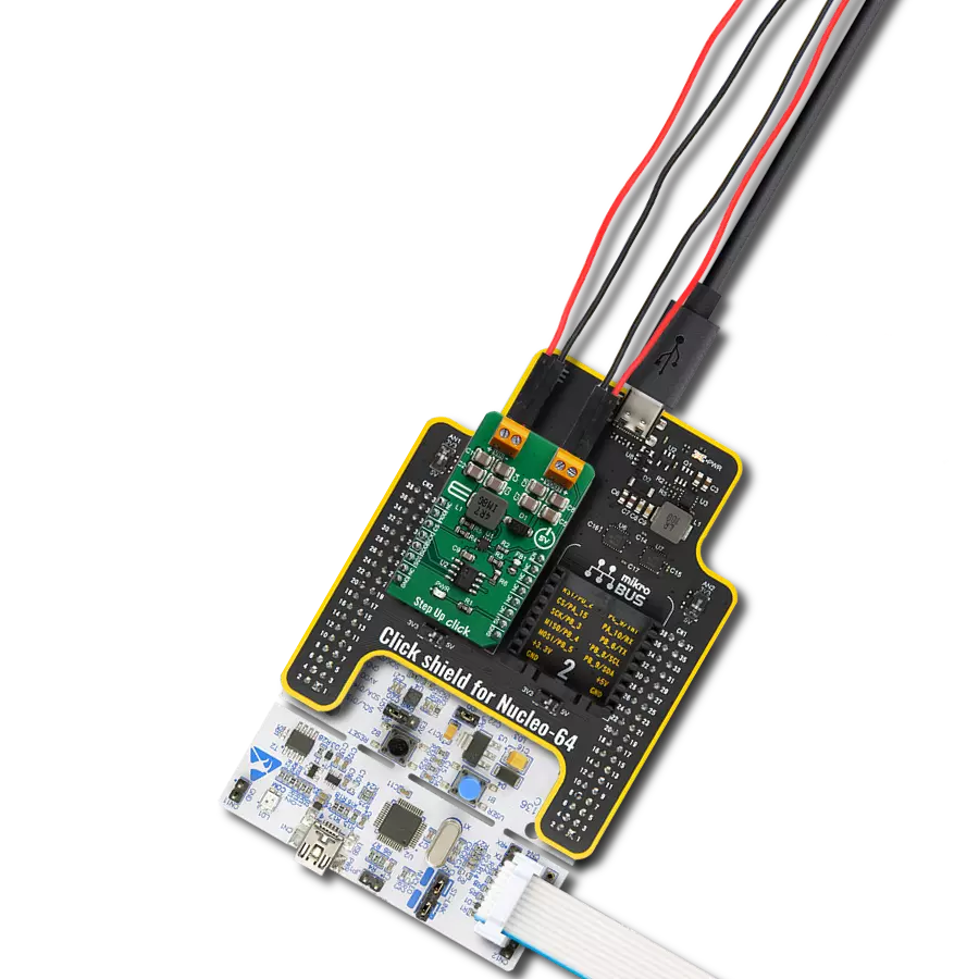
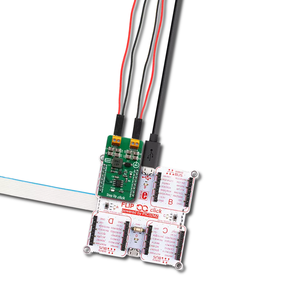
Start by selecting your development board and Click board™. Begin with the Curiosity Nano with PIC18F57Q43 as your development board.


Software Support
Library Description
This library contains API for Boost 11 Click driver.
Key functions:
boost11_active_mode- This function activates the boost operating mode.boost11_read_an_pin_voltage- This function reads results of AD conversion of the AN pin and converts them to proportional voltage level.
Open Source
Code example
The complete application code and a ready-to-use project are available through the NECTO Studio Package Manager for direct installation in the NECTO Studio. The application code can also be found on the MIKROE GitHub account.
/*!
 * @file main.c
 * @brief Boost 11 Click Example.
 *
 * # Description
 * This example demonstrates the use of Boost 11 Click board
 * by controlling the output state.
 *
 * The demo application is composed of two sections :
 *
 * ## Application Init
 * Initialization of GPIO module, log UART, and activate the boost operating mode.
 *
 * ## Application Task
 * The demo application reads measurements of the output voltage level [V].
 * Results are being sent to the UART Terminal, where you can track their changes.
 *
 * @author Nenad Filipovic
 *
 */

#include "board.h"
#include "log.h"
#include "boost11.h"

static boost11_t boost11;   /**< Boost 11 Click driver object. */
static log_t logger;        /**< Logger object. */

void application_init ( void )
{
    log_cfg_t log_cfg;          /**< Logger config object. */
    boost11_cfg_t boost11_cfg;  /**< Click config object. */

    /**
     * Logger initialization.
     * Default baud rate: 115200
     * Default log level: LOG_LEVEL_DEBUG
     * @note If USB_UART_RX and USB_UART_TX
     * are defined as HAL_PIN_NC, you will
     * need to define them manually for log to work.
     * See @b LOG_MAP_USB_UART macro definition for detailed explanation.
     */
    LOG_MAP_USB_UART( log_cfg );
    log_init( &logger, &log_cfg );
    log_info( &logger, " Application Init " );

    // Click initialization.
    boost11_cfg_setup( &boost11_cfg );
    BOOST11_MAP_MIKROBUS( boost11_cfg, MIKROBUS_1 );
    if ( ADC_ERROR == boost11_init( &boost11, &boost11_cfg ) )
    {
        log_error( &logger, " Communication init." );
        for ( ; ; );
    }

    boost11_active_mode( &boost11 );
    Delay_ms ( 100 );

    log_info( &logger, " Application Task " );
}

void application_task ( void )
{
    float voltage = 0;
    if ( BOOST11_OK == boost11_read_an_pin_voltage ( &boost11, &voltage ) )
    {
        log_printf( &logger, " Output Voltage : %.3f[V]\r\n\n", voltage );
        Delay_ms ( 1000 );
    }
}

int main ( void )
{
    /* Do not remove this line or clock might not be set correctly. */
    #ifdef PREINIT_SUPPORTED
    preinit();
    #endif

    application_init( );

    for ( ; ; )
    {
        application_task( );
    }

    return 0;
}

// ------------------------------------------------------------------------ END
Additional Support
Resources
Category:Boost