Unveil the true potential of digital signals using LTC2601 and ATmega328P
Upgrade data understanding with DAC mastery
Published Feb 14, 2024
Click board™
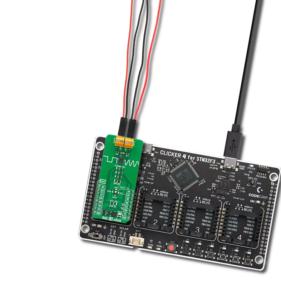
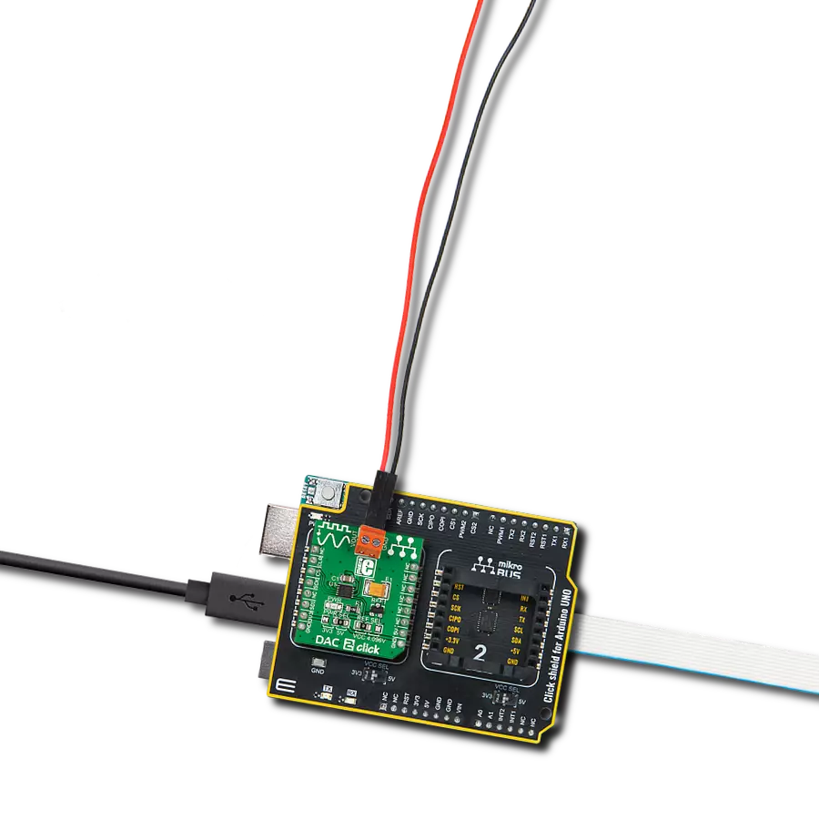
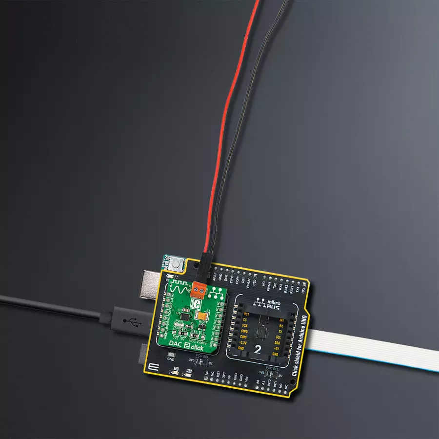
DAC 2 Click
Dev. board
Arduino UNO Rev3
Compiler
NECTO Studio
MCU
ATmega328P
With high accuracy at its core, our solution bridges the gap between digital data and analog interpretation, enhancing your ability to derive meaning and make informed decisions
A
A
Hardware Overview
How does it work?
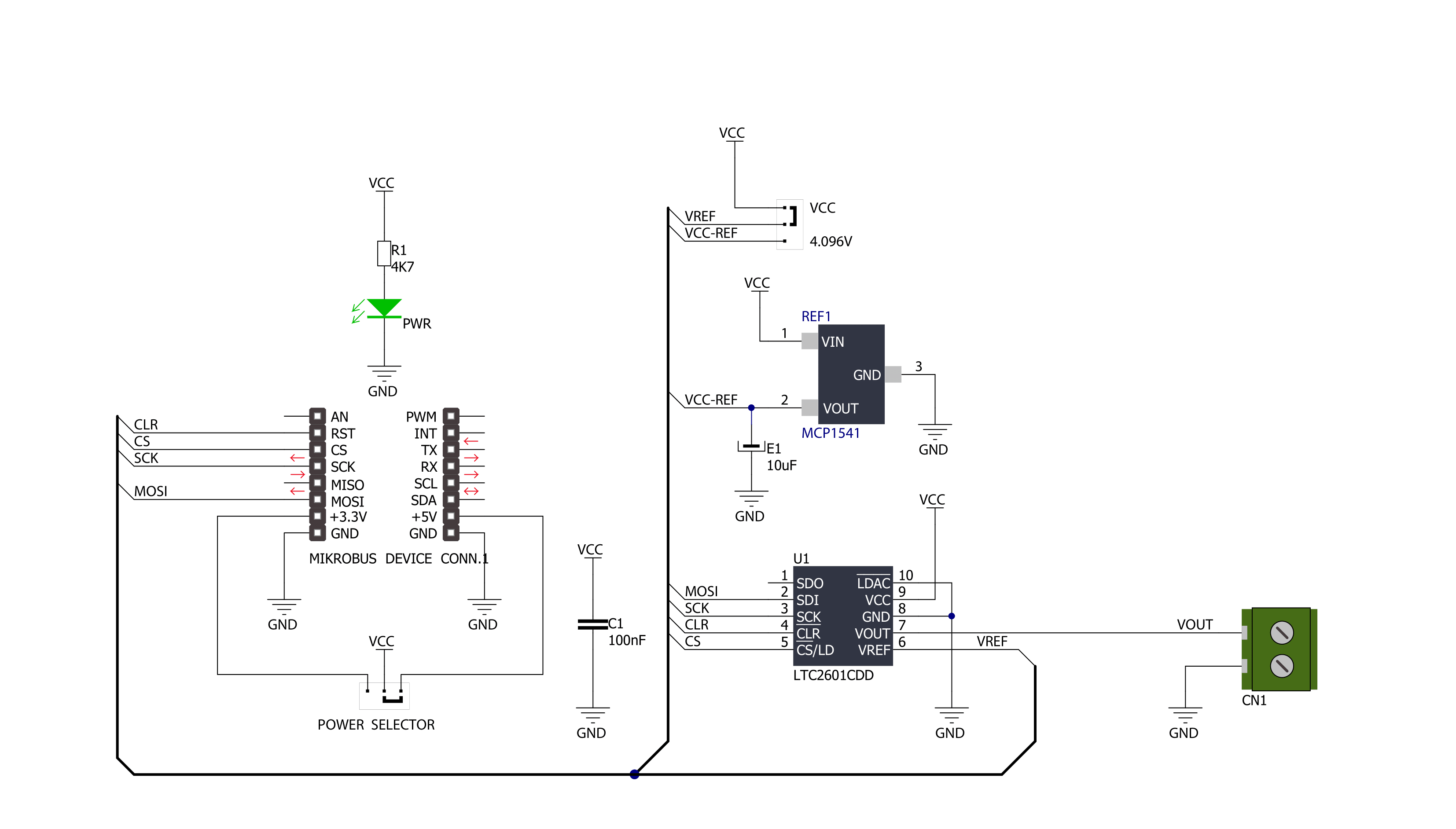
DAC 2 Click is based on the LTC2601, a single 16-bit rail-to-rail voltage output digital-to-analog converter from Analog Devices with built-in high-performance output buffers. The DAC output (VOUT terminal) can directly drive capacitive loads up to 1000pF or current loads up to 15mA and maintains good linearity to within millivolts of both supply rails. The LTC2601's guaranteed monotonic performance is ideal for digital calibration, trim/adjust, and level setting applications in various applications. This Click board™ communicates with MCU through a 3-Wire SPI interface (write-only) with a maximum
frequency of 50MHz. The LTC2601 also provides an asynchronous clear pin routed to the RST pin of the mikroBUS™ socket, which is required in many servo and control applications. A low-level logic at this level-triggered pin clears all registers and causes the DAC voltage outputs to drop to 0V. It also sets all registers to midscale code and causes the DAC voltage outputs to go to midscale. Like any DAC, the MCP3551 uses a reference voltage as the differential voltage range. The reference voltage level selection is performed by positioning the SMD jumper labeled REF SEL to an appropriate position, choosing between 3.3V or 5V
provided by the mikroBUS™ power rails or 4.096V provided by MCP1541. Those voltages may be used as the reference input that results in accuracy and stability. This Click board™ can operate with both 3.3V and 5V logic voltage levels selected via the PWR SEL jumper. This way, both 3.3V and 5V capable MCUs can use the communication lines properly. Also, this Click board™ comes equipped with a library containing easy-to-use functions and an example code that can be used as a reference for further development.

Features overview
Development board
Arduino UNO is a versatile microcontroller board built around the ATmega328P chip. It offers extensive connectivity options for various projects, featuring 14 digital input/output pins, six of which are PWM-capable, along with six analog inputs. Its core components include a 16MHz ceramic resonator, a USB connection, a power jack, an
ICSP header, and a reset button, providing everything necessary to power and program the board. The Uno is ready to go, whether connected to a computer via USB or powered by an AC-to-DC adapter or battery. As the first USB Arduino board, it serves as the benchmark for the Arduino platform, with "Uno" symbolizing its status as the
first in a series. This name choice, meaning "one" in Italian, commemorates the launch of Arduino Software (IDE) 1.0. Initially introduced alongside version 1.0 of the Arduino Software (IDE), the Uno has since become the foundational model for subsequent Arduino releases, embodying the platform's evolution.

Microcontroller Overview
MCU Card / MCU

Architecture
AVR
MCU Memory (KB)
32
Silicon Vendor
Microchip
Pin count
28
RAM (Bytes)
2048
You complete me!
Accessories
Click Shield for Arduino UNO has two proprietary mikroBUS™ sockets, allowing all the Click board™ devices to be interfaced with the Arduino UNO board without effort. The Arduino Uno, a microcontroller board based on the ATmega328P, provides an affordable and flexible way for users to try out new concepts and build prototypes with the ATmega328P microcontroller from various combinations of performance, power consumption, and features. The Arduino Uno has 14 digital input/output pins (of which six can be used as PWM outputs), six analog inputs, a 16 MHz ceramic resonator (CSTCE16M0V53-R0), a USB connection, a power jack, an ICSP header, and reset button. Most of the ATmega328P microcontroller pins are brought to the IO pins on the left and right edge of the board, which are then connected to two existing mikroBUS™ sockets. This Click Shield also has several switches that perform functions such as selecting the logic levels of analog signals on mikroBUS™ sockets and selecting logic voltage levels of the mikroBUS™ sockets themselves. Besides, the user is offered the possibility of using any Click board™ with the help of existing bidirectional level-shifting voltage translators, regardless of whether the Click board™ operates at a 3.3V or 5V logic voltage level. Once you connect the Arduino UNO board with our Click Shield for Arduino UNO, you can access hundreds of Click boards™, working with 3.3V or 5V logic voltage levels.

Used MCU Pins
mikroBUS™ mapper
Take a closer look
Click board™ Schematic
Step by step
Project assembly

Start by selecting your development board and Click board™. Begin with the Arduino UNO Rev3 as your development board.


Track your results in real time
Application Output
1. Application Output - In Debug mode, the 'Application Output' window enables real-time data monitoring, offering direct insight into execution results. Ensure proper data display by configuring the environment correctly using the provided tutorial.

2. UART Terminal - Use the UART Terminal to monitor data transmission via a USB to UART converter, allowing direct communication between the Click board™ and your development system. Configure the baud rate and other serial settings according to your project's requirements to ensure proper functionality. For step-by-step setup instructions, refer to the provided tutorial.

3. Plot Output - The Plot feature offers a powerful way to visualize real-time sensor data, enabling trend analysis, debugging, and comparison of multiple data points. To set it up correctly, follow the provided tutorial, which includes a step-by-step example of using the Plot feature to display Click board™ readings. To use the Plot feature in your code, use the function: plot(*insert_graph_name*, variable_name);. This is a general format, and it is up to the user to replace 'insert_graph_name' with the actual graph name and 'variable_name' with the parameter to be displayed.

Software Support
Library Description
This library contains API for DAC 2 Click driver.
Key functions:
dac2_default_cfg- This function executes default configuration for LTC2601dac2_write_output_voltage_procentage- This function required percentage value ( from 0% to 100% ) convert to digital input and transforms it to the output voltage from 0 to Vref [mV]
Open Source
Code example
The complete application code and a ready-to-use project are available through the NECTO Studio Package Manager for direct installation in the NECTO Studio. The application code can also be found on the MIKROE GitHub account.
/*!
 * \file
 * \brief Dac2 Click example
 *
 * # Description
 * DAC 2 Click represents a 16-bit digital-to-analog converter.
 *
 * The demo application is composed of two sections :
 *
 * ## Application Init
 * Application Init performs Logger and Click initialization.
 *
 * ## Application Task
 * This example of the DAC 2 communicates with MCU through the SPI communication,
 * send digital input ( form 0 to 100 with step 1 ) and transforms it
 * to the output voltage, ranging from 0 to Vref [mV].
 *
 * \author Mihajlo Djordjevic
 *
 */
// ------------------------------------------------------------------- INCLUDES

#include "board.h"
#include "log.h"
#include "dac2.h"

// ------------------------------------------------------------------ VARIABLES

static dac2_t dac2;
static log_t logger;

// ------------------------------------------------------ APPLICATION FUNCTIONS

void application_init ( void )
{
    log_cfg_t log_cfg;
    dac2_cfg_t cfg;

    /**
     * Logger initialization.
     * Default baud rate: 115200
     * Default log level: LOG_LEVEL_DEBUG
     * @note If USB_UART_RX and USB_UART_TX
     * are defined as HAL_PIN_NC, you will
     * need to define them manually for log to work.
     * See @b LOG_MAP_USB_UART macro definition for detailed explanation.
     */
    LOG_MAP_USB_UART( log_cfg );
    log_init( &logger, &log_cfg );
    log_info( &logger, "---- Application Init ----" );
    Delay_ms ( 1000 );

    //  Click initialization.

    dac2_cfg_setup( &cfg );
    DAC2_MAP_MIKROBUS( cfg, MIKROBUS_1 );
    dac2_init( &dac2, &cfg );

    log_printf( &logger, "--------------------------\r\n" );
    log_printf( &logger, " ----- DAC 2  Click ----- \r\n" );
    log_printf( &logger, "--------------------------\r\n" );
    Delay_ms ( 1000 );

    dac2_default_cfg( &dac2 );
    Delay_ms ( 1000 );

    log_printf( &logger, " -- Initialization done --\r\n" );
    log_printf( &logger, "--------------------------\r\n" );
    Delay_ms ( 1000 );
}

void application_task ( void )
{
    uint16_t voltage_out;
    uint8_t value_pct;

    for ( value_pct = 0; value_pct <= 100; value_pct += 10 )
    {
        dac2_write_output_voltage_procentage( &dac2, value_pct );
        voltage_out = value_pct * 50;
        log_printf( &logger, "Voltage Output: %d mV\r\n", voltage_out );

        voltage_out = value_pct;
        log_printf( &logger, "Percentage Output: %d %%\r\n", voltage_out );

        log_printf( &logger, "--------------------------\r\n" );
        Delay_ms ( 1000 );
        Delay_ms ( 1000 );
        Delay_ms ( 1000 );
        Delay_ms ( 1000 );
        Delay_ms ( 1000 );
    }

    log_printf( &logger, "###############################\r\n" );
    Delay_ms ( 1000 );
}

int main ( void )
{
    /* Do not remove this line or clock might not be set correctly. */
    #ifdef PREINIT_SUPPORTED
    preinit();
    #endif

    application_init( );

    for ( ; ; )
    {
        application_task( );
    }

    return 0;
}

// ------------------------------------------------------------------------ END
Additional Support
Resources
Category:DAC