Create projects with rapid boot times and extensive low-power data storage capabilities using AT25EU0041A and STM32L073RZ
4Mbit serial flash memory suitable for battery-powered or energy-sensitive applications

Published Mar 12, 2024
Click board™
Flash 12 Click
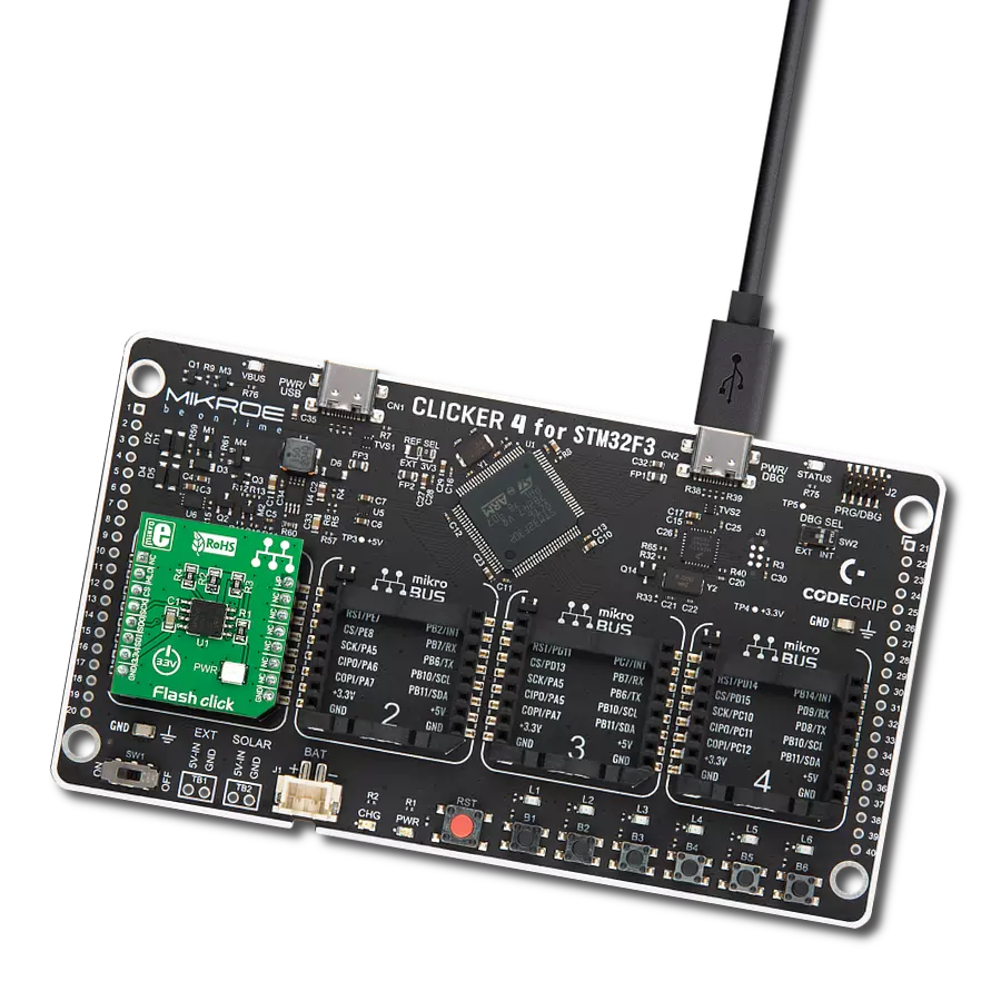
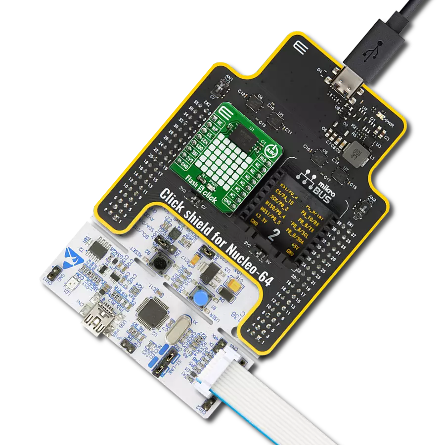
Dev. board
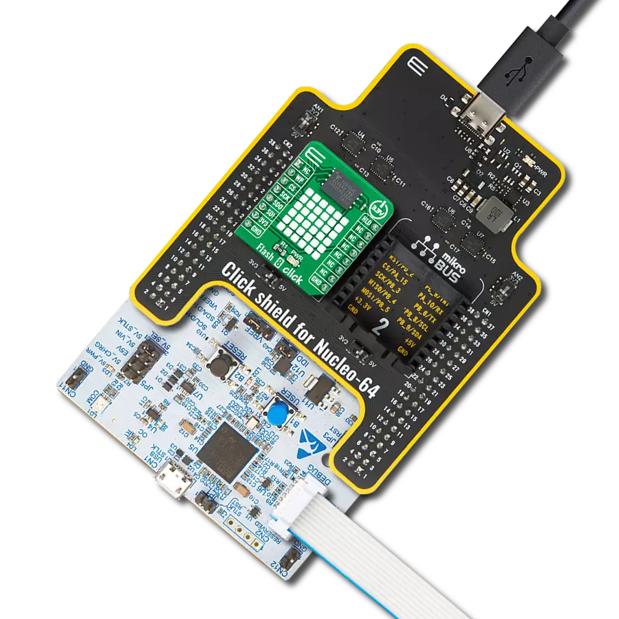
Nucleo-64 with STM32L073RZ MCU
Compiler
NECTO Studio
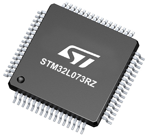
MCU
STM32L073RZ
Ultra-low power consumption, fast erase times, and the ability to execute code directly from memory makes it an excellent choice for developers looking to optimize their projects for the edge of IoT networks
A
A
Hardware Overview
How does it work?
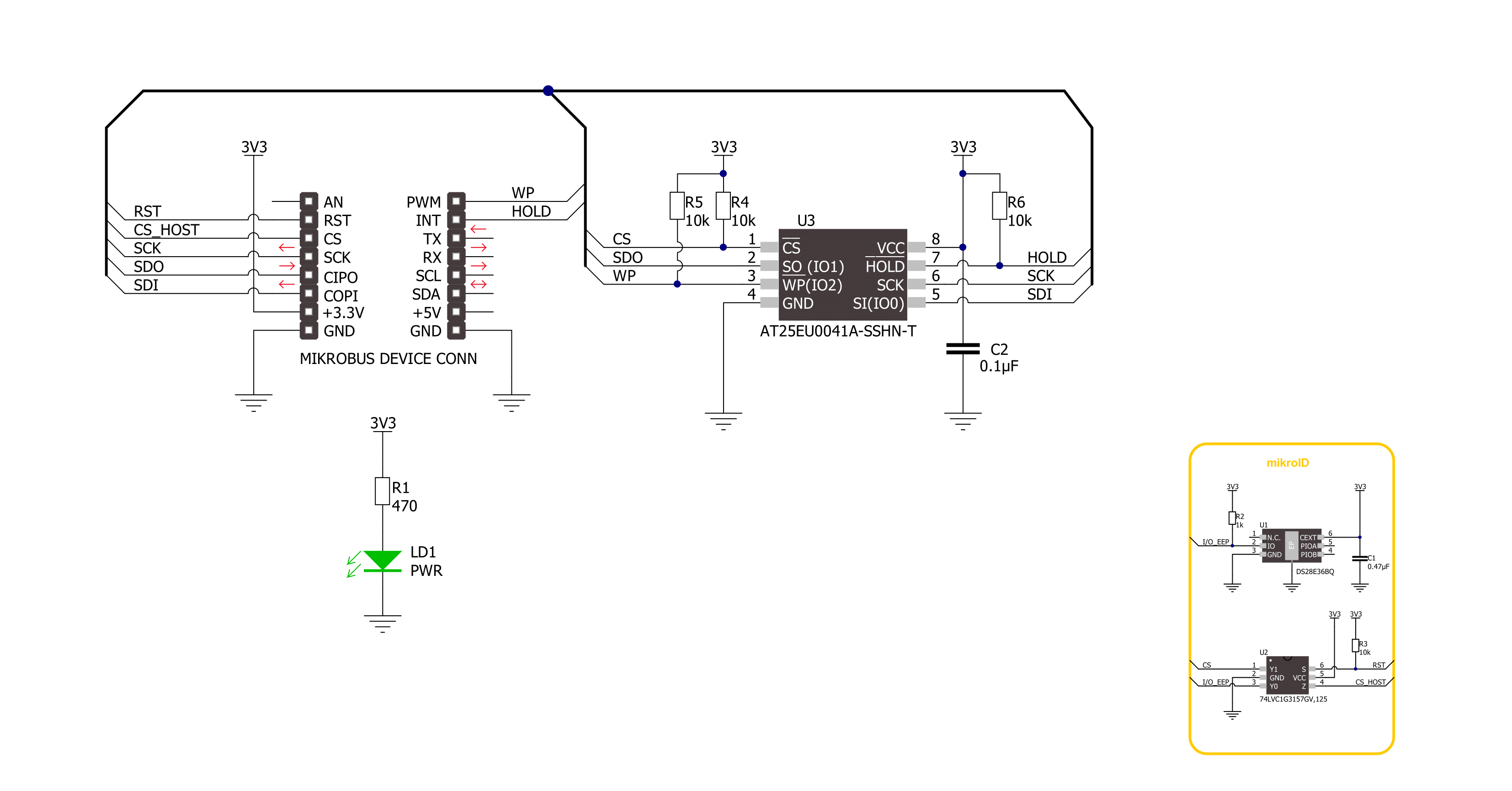
Flash 12 Click is based on the AT25EU0041A, a 4Mbit serial flash memory from Renesas, known for its ultra-low power consumption. This memory is part of a series specifically developed for applications operating on the IoT network's fringes, where energy efficiency is paramount. The AT25EU0041A is particularly well-suited for battery-operated systems, offering a reliable solution for both program code storage, which is then loaded into embedded systems, and serving as external RAM for direct program execution from the NOR Flash memory. Based on these features, this Click board™ is ideal for various applications from low-power reading and rapid erasure to boot/code shadow memory and straightforward event/data logging. The AT25EU0041A sets a new standard in energy efficiency through its innovative erase architecture, which features short erase times while maintaining low power consumption across all
operations, including reading, programming, and erasing. The consistent erase times, irrespective of the memory block size, and a page-erase capability that allows for as little as 256 bytes to be erased enhance the efficiency of write operations. Moreover, the AT25EU0041A adheres to the JEDEC standard for manufacturer and device identification, and it includes a 128-bit unique serial number, further enhancing its utility and security features. Flash 12 Click communicates with MCU through a standard SPI interface supporting the two most common SPI modes, SPI Mode 0 and 3, and a maximum clock frequency of up to 108MHz. The AT25EU0041A enhances data transfer rates through Dual and Quad SPI operations, which double and quadruple the standard SPI speed, respectively. These enhanced speeds are achieved by re-purposing the SI and SO pins as bidirectional I/O pins during Dual and Quad SPI operations.
Furthermore, the board features a HOLD function, marked as HLD and routed on the default position of the INT pin of the mikroBUS™ socket. The hold function allows the suspension of serial communications without disrupting ongoing operations. The board also has a Write Protect feature, marked as WP and routed on the default position of the PWM of the mikroBUS™ socket, that safeguards all registers and memory from unintended write operations through both hardware and software mechanisms. This Click board™ can be operated only with a 3.3V logic voltage level. The board must perform appropriate logic voltage level conversion before using MCUs with different logic levels. Also, it comes equipped with a library containing functions and an example code that can be used as a reference for further development.

Features overview
Development board
Nucleo-64 with STM32L073RZ MCU offers a cost-effective and adaptable platform for developers to explore new ideas and prototype their designs. This board harnesses the versatility of the STM32 microcontroller, enabling users to select the optimal balance of performance and power consumption for their projects. It accommodates the STM32 microcontroller in the LQFP64 package and includes essential components such as a user LED, which doubles as an ARDUINO® signal, alongside user and reset push-buttons, and a 32.768kHz crystal oscillator for precise timing operations. Designed with expansion and flexibility in mind, the Nucleo-64 board features an ARDUINO® Uno V3 expansion connector and ST morpho extension pin
headers, granting complete access to the STM32's I/Os for comprehensive project integration. Power supply options are adaptable, supporting ST-LINK USB VBUS or external power sources, ensuring adaptability in various development environments. The board also has an on-board ST-LINK debugger/programmer with USB re-enumeration capability, simplifying the programming and debugging process. Moreover, the board is designed to simplify advanced development with its external SMPS for efficient Vcore logic supply, support for USB Device full speed or USB SNK/UFP full speed, and built-in cryptographic features, enhancing both the power efficiency and security of projects. Additional connectivity is
provided through dedicated connectors for external SMPS experimentation, a USB connector for the ST-LINK, and a MIPI® debug connector, expanding the possibilities for hardware interfacing and experimentation. Developers will find extensive support through comprehensive free software libraries and examples, courtesy of the STM32Cube MCU Package. This, combined with compatibility with a wide array of Integrated Development Environments (IDEs), including IAR Embedded Workbench®, MDK-ARM, and STM32CubeIDE, ensures a smooth and efficient development experience, allowing users to fully leverage the capabilities of the Nucleo-64 board in their projects.

Microcontroller Overview
MCU Card / MCU
Architecture
ARM Cortex-M0
MCU Memory (KB)
192
Silicon Vendor
STMicroelectronics
Pin count
64
RAM (Bytes)
20480
You complete me!
Accessories
Click Shield for Nucleo-64 comes equipped with two proprietary mikroBUS™ sockets, allowing all the Click board™ devices to be interfaced with the STM32 Nucleo-64 board with no effort. This way, Mikroe allows its users to add any functionality from our ever-growing range of Click boards™, such as WiFi, GSM, GPS, Bluetooth, ZigBee, environmental sensors, LEDs, speech recognition, motor control, movement sensors, and many more. More than 1537 Click boards™, which can be stacked and integrated, are at your disposal. The STM32 Nucleo-64 boards are based on the microcontrollers in 64-pin packages, a 32-bit MCU with an ARM Cortex M4 processor operating at 84MHz, 512Kb Flash, and 96KB SRAM, divided into two regions where the top section represents the ST-Link/V2 debugger and programmer while the bottom section of the board is an actual development board. These boards are controlled and powered conveniently through a USB connection to program and efficiently debug the Nucleo-64 board out of the box, with an additional USB cable connected to the USB mini port on the board. Most of the STM32 microcontroller pins are brought to the IO pins on the left and right edge of the board, which are then connected to two existing mikroBUS™ sockets. This Click Shield also has several switches that perform functions such as selecting the logic levels of analog signals on mikroBUS™ sockets and selecting logic voltage levels of the mikroBUS™ sockets themselves. Besides, the user is offered the possibility of using any Click board™ with the help of existing bidirectional level-shifting voltage translators, regardless of whether the Click board™ operates at a 3.3V or 5V logic voltage level. Once you connect the STM32 Nucleo-64 board with our Click Shield for Nucleo-64, you can access hundreds of Click boards™, working with 3.3V or 5V logic voltage levels.

Used MCU Pins
mikroBUS™ mapper
Take a closer look
Click board™ Schematic
Step by step
Project assembly
Start by selecting your development board and Click board™. Begin with the Nucleo-64 with STM32L073RZ MCU as your development board.


Track your results in real time
Application Output
1. Application Output - In Debug mode, the 'Application Output' window enables real-time data monitoring, offering direct insight into execution results. Ensure proper data display by configuring the environment correctly using the provided tutorial.

2. UART Terminal - Use the UART Terminal to monitor data transmission via a USB to UART converter, allowing direct communication between the Click board™ and your development system. Configure the baud rate and other serial settings according to your project's requirements to ensure proper functionality. For step-by-step setup instructions, refer to the provided tutorial.

3. Plot Output - The Plot feature offers a powerful way to visualize real-time sensor data, enabling trend analysis, debugging, and comparison of multiple data points. To set it up correctly, follow the provided tutorial, which includes a step-by-step example of using the Plot feature to display Click board™ readings. To use the Plot feature in your code, use the function: plot(*insert_graph_name*, variable_name);. This is a general format, and it is up to the user to replace 'insert_graph_name' with the actual graph name and 'variable_name' with the parameter to be displayed.

Software Support
Library Description
This library contains API for Flash 12 Click driver.
Key functions:
flash12_memory_write- This function writes a desired number of data bytes starting to the selected memory address by using SPI serial interfaceflash12_memory_read- This function reads a desired number of data bytes starting from the selected memory address by using SPI serial interfaceflash12_erase_memory- This function erases the selected amount of memory which contains the selected address
Open Source
Code example
The complete application code and a ready-to-use project are available through the NECTO Studio Package Manager for direct installation in the NECTO Studio. The application code can also be found on the MIKROE GitHub account.
/*!
 * @file main.c
 * @brief Flash 12 Click example
 *
 * # Description
 * This example demonstrates the use of Flash 12 Click board
 * by writing specified data to the memory and reading it back.
 *
 * The demo application is composed of two sections :
 *
 * ## Application Init
 * The initialization of SPI module and log UART.
 * After driver initialization, the app sets the default configuration.
 *
 * ## Application Task
 * The demo application writes a desired number of bytes to the memory
 * and then verifies if it is written correctly by reading
 * from the same memory location and displaying the memory content.
 * Results are being sent to the UART Terminal, where you can track their changes.
 *
 * @author Nenad Filipovic
 *
 */

#include "board.h"
#include "log.h"
#include "flash12.h"

// Starting memory address
#define STARTING_ADDRESS            0x012345

// Demo text messages
#define DEMO_TEXT_MESSAGE_1         "MikroE"
#define DEMO_TEXT_MESSAGE_2         "Flash 12 Click"

static flash12_t flash12;
static log_t logger;

void application_init ( void )
{
    log_cfg_t log_cfg;  /**< Logger config object. */
    flash12_cfg_t flash12_cfg;  /**< Click config object. */

    /**
     * Logger initialization.
     * Default baud rate: 115200
     * Default log level: LOG_LEVEL_DEBUG
     * @note If USB_UART_RX and USB_UART_TX
     * are defined as HAL_PIN_NC, you will
     * need to define them manually for log to work.
     * See @b LOG_MAP_USB_UART macro definition for detailed explanation.
     */
    LOG_MAP_USB_UART( log_cfg );
    log_init( &logger, &log_cfg );
    log_info( &logger, " Application Init " );

    // Click initialization.
    flash12_cfg_setup( &flash12_cfg );
    FLASH12_MAP_MIKROBUS( flash12_cfg, MIKROBUS_1 );
    if ( SPI_MASTER_ERROR == flash12_init( &flash12, &flash12_cfg ) )
    {
        log_error( &logger, " Communication init." );
        for ( ; ; );
    }

    if ( FLASH12_ERROR == flash12_default_cfg ( &flash12 ) )
    {
        log_error( &logger, " Default configuration." );
        for ( ; ; );
    }

    log_info( &logger, " Application Task\r\n" );
}

void application_task ( void )
{
    uint8_t data_buf[ 128 ] = { 0 };

    log_printf( &logger, " Memory address: 0x%.6LX\r\n", ( uint32_t ) STARTING_ADDRESS );
    if ( FLASH12_OK == flash12_erase_memory( &flash12, FLASH12_CMD_BLOCK_ERASE_4KB, STARTING_ADDRESS ) )
    {
        log_printf( &logger, " Erase memory block (4KB)\r\n" );
    }
    memcpy( data_buf, DEMO_TEXT_MESSAGE_1, strlen( DEMO_TEXT_MESSAGE_1 ) );
    if ( FLASH12_OK == flash12_memory_write( &flash12, STARTING_ADDRESS,
                                                       data_buf,
                                                       sizeof( data_buf ) ) )
    {
        log_printf( &logger, " Write data: %s\r\n", data_buf );
        Delay_ms ( 100 );
    }

    memset( data_buf, 0, sizeof( data_buf ) );
    if ( FLASH12_OK == flash12_memory_read( &flash12, STARTING_ADDRESS,
                                                      data_buf,
                                                      sizeof( data_buf ) ) )
    {
        log_printf( &logger, " Read data: %s\r\n\n", data_buf );
        Delay_ms ( 1000 );
        Delay_ms ( 1000 );
        Delay_ms ( 1000 );
    }

    log_printf( &logger, " Memory address: 0x%.6LX\r\n", ( uint32_t ) STARTING_ADDRESS );
    if ( FLASH12_OK == flash12_erase_memory( &flash12, FLASH12_CMD_BLOCK_ERASE_4KB, STARTING_ADDRESS ) )
    {
        log_printf( &logger, " Erase memory block (4KB)\r\n" );
    }
    memcpy( data_buf, DEMO_TEXT_MESSAGE_2, strlen( DEMO_TEXT_MESSAGE_2 ) );
    if ( FLASH12_OK == flash12_memory_write( &flash12, STARTING_ADDRESS,
                                             data_buf, sizeof( data_buf ) ) )
    {
        log_printf( &logger, " Write data: %s\r\n", data_buf );
        Delay_ms ( 100 );
    }
    memset( data_buf, 0, sizeof ( data_buf ) );
    if ( FLASH12_OK == flash12_memory_read( &flash12, STARTING_ADDRESS,
                                            data_buf, sizeof ( data_buf ) ) )
    {
        log_printf( &logger, " Read data: %s\r\n\n", data_buf );
        Delay_ms ( 1000 );
        Delay_ms ( 1000 );
        Delay_ms ( 1000 );
    }
}

int main ( void )
{
    /* Do not remove this line or clock might not be set correctly. */
    #ifdef PREINIT_SUPPORTED
    preinit();
    #endif

    application_init( );

    for ( ; ; )
    {
        application_task( );
    }

    return 0;
}

// ------------------------------------------------------------------------ END
Additional Support
Resources
Category:FLASH