Bipolar voltage booster made easy with LT3582 and STM32F091RC
Dual voltage dynamo

Published Feb 26, 2024
Click board™
Boost-INV Click
Dev. board
Nucleo-64 with STM32F091RC MCU
Compiler
NECTO Studio
MCU
STM32F091RC
From positive to negative, we've got your voltage covered!
A
A
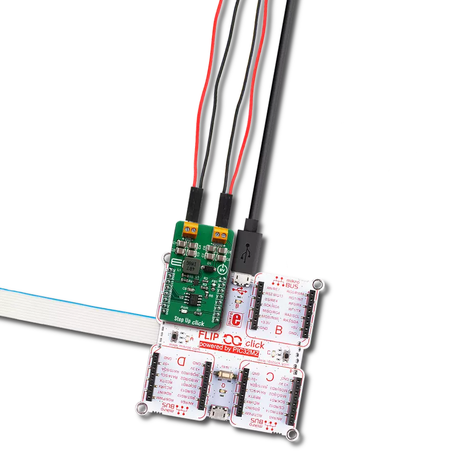
Hardware Overview
How does it work?
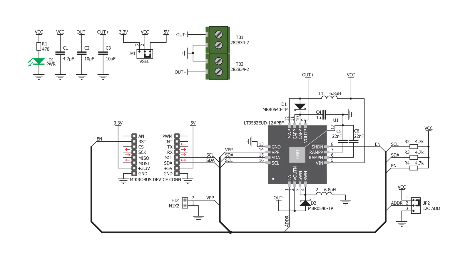
Boost-INV Click is based on the LT3582, a programmable boost and inverting DC/DC converter with OTP memory from Analog Devices. This IC is a dual circuit, offering a boost DC/DC converter and an inverter in one package. The boost converter can provide up to 12.78V on the output while driving the load with up to 350mA. The inverter can provide -13.95V, offering up to 600mA to the connected load, before the current limiting is activated. The boost converter uses an advanced switching scheme with the source-grounded NMOS as the main switching element, controlling the off-time and the peak current. The programmable voltage divider on the output provides the feedback voltage needed for the regulation. The inverter topology allows a single inductor to be used on the output, simplifying the design. As mentioned, the LT3582 features programmable parameters, which can be accessed via the I2C interface. These parameters include configuring the output voltages, power sequencing, and output voltage ramp rates. An onboard OTP non-volatile memory can be programmed with values that will be used at the startup. The command register (CMDR) is reset to 0x00h upon powering up, which turns off the outputs and sets the device to read parameters
stored in the OTP area. If the OTP memory area is empty, it is necessary to set up working parameters first (output voltage, power-up sequence, charging current for the ramp-up capacitors, and more) before using the device. It is worth mentioning that there are three bits in the CMDR register, referred to as RSEL0, RSEL1, and RSEL2 in the LT3582 datasheet, which redirects the device to use either registers or the OTP memory. When set to 0, the device uses parameters stored in the OTP memory. Note that 0x00h is the default value of the CMDR register, meaning settings stored in the OTP will be used by default after powering on. It is possible to dynamically change the values of the output voltages and other configurable working parameters. However, turning off the device (SWOFF bit of the CMDR register) is highly recommended before modifying working parameters since large output voltage changes can cause large current spikes on the switching circuitry if performed in real time while the switching circuit is running. Programming the OTP requires an external power source, which is fairly filtered (possibly with a filtering capacitor on the output). Voltage drop under 13V might trigger the FAULT bit and render the device unusable.
This voltage ranges from 13V to 15V. The Click board™ has the standard 2.54mm (100mil) header. Once the programming voltage is connected (VPP pad), the WOTP bit of the CMDR register initiates the programming. The complete algorithm with a detailed description of the OTP programming procedure can be found in the LT3582 datasheet. An onboard SMD jumper labeled as VSEL allows selection between the 3.3V and 5V power rail from mikroBUS™, routing it to the voltage input pin of the LT3582 IC. The I2C pull-up resistors are also connected to this voltage, allowing communication with both 3.3V and 5V MCUs. The Click board™ also offers the I2C address selection jumper, labeled as the I2C ADD. This jumper selects between two possible 7-bit addresses: the left position sets the I2C slave address to 0x49h, while the right position sets the address to 0x69h. Note that this is the 7-bit address only - to get the complete I2C address, an R/W bit needs to be added at the end. Input screw terminals allow secure connection for the load and are clearly labeled to avoid confusion: the V- pin offers the negative voltage, while the V+ pin outputs positive voltage. GND pins are connected to the common ground of the Click board™.

Features overview
Development board
Nucleo-64 with STM32F091RC MCU offers a cost-effective and adaptable platform for developers to explore new ideas and prototype their designs. This board harnesses the versatility of the STM32 microcontroller, enabling users to select the optimal balance of performance and power consumption for their projects. It accommodates the STM32 microcontroller in the LQFP64 package and includes essential components such as a user LED, which doubles as an ARDUINO® signal, alongside user and reset push-buttons, and a 32.768kHz crystal oscillator for precise timing operations. Designed with expansion and flexibility in mind, the Nucleo-64 board features an ARDUINO® Uno V3 expansion connector and ST morpho extension pin
headers, granting complete access to the STM32's I/Os for comprehensive project integration. Power supply options are adaptable, supporting ST-LINK USB VBUS or external power sources, ensuring adaptability in various development environments. The board also has an on-board ST-LINK debugger/programmer with USB re-enumeration capability, simplifying the programming and debugging process. Moreover, the board is designed to simplify advanced development with its external SMPS for efficient Vcore logic supply, support for USB Device full speed or USB SNK/UFP full speed, and built-in cryptographic features, enhancing both the power efficiency and security of projects. Additional connectivity is
provided through dedicated connectors for external SMPS experimentation, a USB connector for the ST-LINK, and a MIPI® debug connector, expanding the possibilities for hardware interfacing and experimentation. Developers will find extensive support through comprehensive free software libraries and examples, courtesy of the STM32Cube MCU Package. This, combined with compatibility with a wide array of Integrated Development Environments (IDEs), including IAR Embedded Workbench®, MDK-ARM, and STM32CubeIDE, ensures a smooth and efficient development experience, allowing users to fully leverage the capabilities of the Nucleo-64 board in their projects.

Microcontroller Overview
MCU Card / MCU

Architecture
ARM Cortex-M0
MCU Memory (KB)
256
Silicon Vendor
STMicroelectronics
Pin count
64
RAM (Bytes)
32768
You complete me!
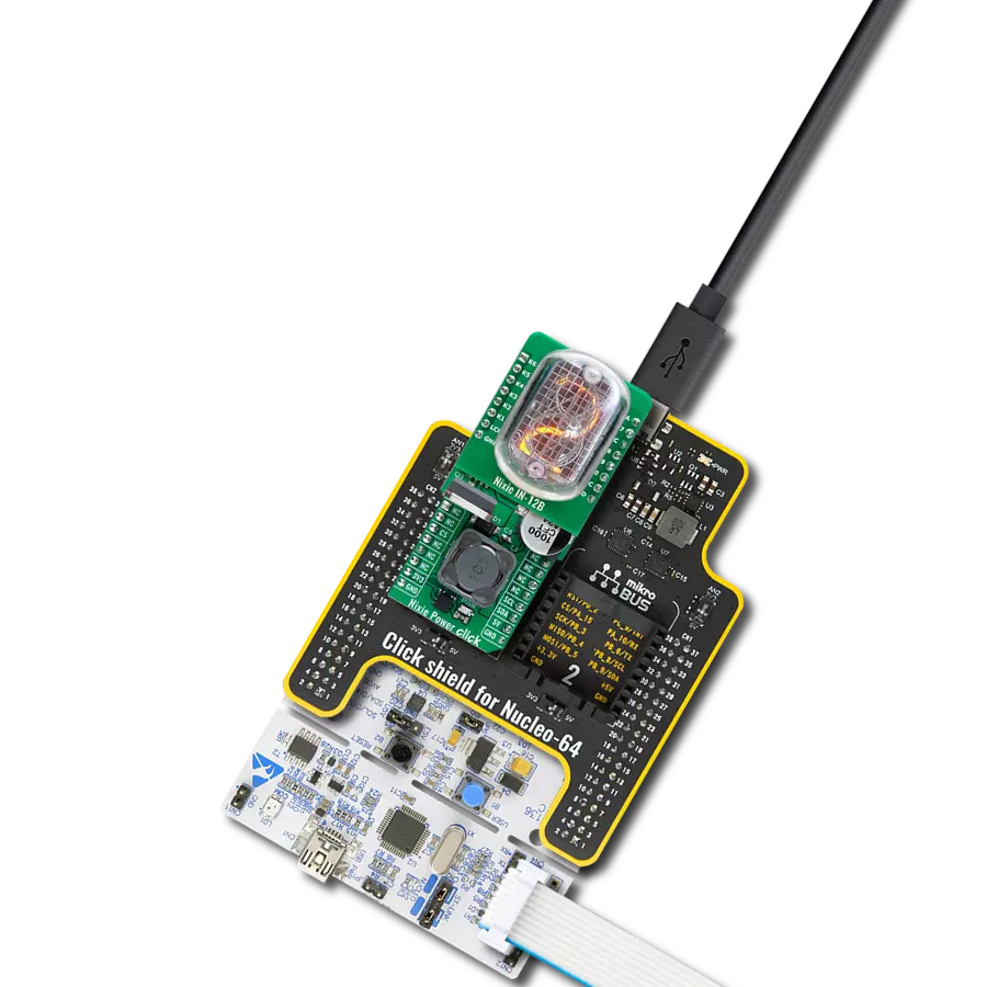
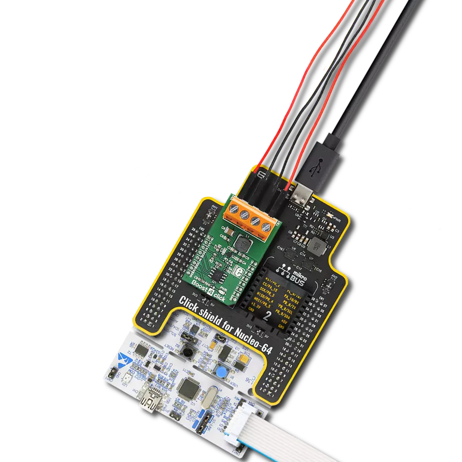
Accessories
Click Shield for Nucleo-64 comes equipped with two proprietary mikroBUS™ sockets, allowing all the Click board™ devices to be interfaced with the STM32 Nucleo-64 board with no effort. This way, Mikroe allows its users to add any functionality from our ever-growing range of Click boards™, such as WiFi, GSM, GPS, Bluetooth, ZigBee, environmental sensors, LEDs, speech recognition, motor control, movement sensors, and many more. More than 1537 Click boards™, which can be stacked and integrated, are at your disposal. The STM32 Nucleo-64 boards are based on the microcontrollers in 64-pin packages, a 32-bit MCU with an ARM Cortex M4 processor operating at 84MHz, 512Kb Flash, and 96KB SRAM, divided into two regions where the top section represents the ST-Link/V2 debugger and programmer while the bottom section of the board is an actual development board. These boards are controlled and powered conveniently through a USB connection to program and efficiently debug the Nucleo-64 board out of the box, with an additional USB cable connected to the USB mini port on the board. Most of the STM32 microcontroller pins are brought to the IO pins on the left and right edge of the board, which are then connected to two existing mikroBUS™ sockets. This Click Shield also has several switches that perform functions such as selecting the logic levels of analog signals on mikroBUS™ sockets and selecting logic voltage levels of the mikroBUS™ sockets themselves. Besides, the user is offered the possibility of using any Click board™ with the help of existing bidirectional level-shifting voltage translators, regardless of whether the Click board™ operates at a 3.3V or 5V logic voltage level. Once you connect the STM32 Nucleo-64 board with our Click Shield for Nucleo-64, you can access hundreds of Click boards™, working with 3.3V or 5V logic voltage levels.

Used MCU Pins
mikroBUS™ mapper
Take a closer look
Click board™ Schematic
Step by step
Project assembly
Start by selecting your development board and Click board™. Begin with the Nucleo-64 with STM32F091RC MCU as your development board.


Track your results in real time
Application Output
1. Application Output - In Debug mode, the 'Application Output' window enables real-time data monitoring, offering direct insight into execution results. Ensure proper data display by configuring the environment correctly using the provided tutorial.

2. UART Terminal - Use the UART Terminal to monitor data transmission via a USB to UART converter, allowing direct communication between the Click board™ and your development system. Configure the baud rate and other serial settings according to your project's requirements to ensure proper functionality. For step-by-step setup instructions, refer to the provided tutorial.

3. Plot Output - The Plot feature offers a powerful way to visualize real-time sensor data, enabling trend analysis, debugging, and comparison of multiple data points. To set it up correctly, follow the provided tutorial, which includes a step-by-step example of using the Plot feature to display Click board™ readings. To use the Plot feature in your code, use the function: plot(*insert_graph_name*, variable_name);. This is a general format, and it is up to the user to replace 'insert_graph_name' with the actual graph name and 'variable_name' with the parameter to be displayed.

Software Support
Library Description
This library contains API for Boost-INV Click driver.
Key functions:
boostinv_enable- Functions for enable chipboostinv_set_positive_voltage- Functions for set positive output voltageboostinv_set_negative_voltage- Functions for set negative output voltage
Open Source
Code example
The complete application code and a ready-to-use project are available through the NECTO Studio Package Manager for direct installation in the NECTO Studio. The application code can also be found on the MIKROE GitHub account.
/*!
 * \file
 * \brief BoostInv Click example
 *
 * # Description
 * Changes the positive and negative output voltage. Input Voltage 3.3V.
 * Positive output voltage goes from 3200mV, 7750mV, 12000mV and 7750mV.
 * Negative output voltage goes from -1450mV, -6700mV, -11050mV and -6700mV.
 *
 * The demo application is composed of two sections :
 *
 * ## Application Init
 * Initializes I2C module and sets EN ( RST ) pin as output.
 *
 * ## Application Task
 * Changes the positive and negative output voltage every 5 sec.
 *
 * \author Luka FIlipovic
 *
 */
// ------------------------------------------------------------------- INCLUDES

#include "board.h"
#include "log.h"
#include "boostinv.h"

// ------------------------------------------------------------------ VARIABLES

static boostinv_t boostinv;
static log_t logger;

// ------------------------------------------------------ APPLICATION FUNCTIONS

void application_init ( void )
{
    log_cfg_t log_cfg;
    boostinv_cfg_t cfg;

    /**
     * Logger initialization.
     * Default baud rate: 115200
     * Default log level: LOG_LEVEL_DEBUG
     * @note If USB_UART_RX and USB_UART_TX
     * are defined as HAL_PIN_NC, you will
     * need to define them manually for log to work.
     * See @b LOG_MAP_USB_UART macro definition for detailed explanation.
     */
    LOG_MAP_USB_UART( log_cfg );
    log_init( &logger, &log_cfg );
    log_info( &logger, "---- Application Init ----" );

    //  Click initialization.

    boostinv_cfg_setup( &cfg );
    BOOSTINV_MAP_MIKROBUS( cfg, MIKROBUS_1 );
    boostinv_init( &boostinv, &cfg );

    boostinv_default_cfg ( &boostinv );
    log_printf( &logger, "     Boost INV Click\r\n" );
    log_printf( &logger, "-------------------------\r\n" );
    Delay_ms ( 100 );
}

void application_task ( void )
{
    // Sets Positive output voltage

    log_printf( &logger, " Positive output voltage \r\n" );
    log_printf( &logger, "- - - - - - - - - - - - -\r\n" );
    log_printf( &logger, "          3200 mV\r\n" );
    log_printf( &logger, "-------------------------\r\n" );
    boostinv_set_positive_voltage( &boostinv, BOOSTINV_VOLTAGE_POSITIVE_3200_mV );
    Delay_ms ( 1000 );
    Delay_ms ( 1000 );
    Delay_ms ( 1000 );
    Delay_ms ( 1000 );
    Delay_ms ( 1000 );

    log_printf( &logger, "          7750 mV\r\n" );
    log_printf( &logger, "-------------------------\r\n" );
    boostinv_set_positive_voltage( &boostinv, BOOSTINV_VOLTAGE_POSITIVE_7750_mV );
    Delay_ms ( 1000 );
    Delay_ms ( 1000 );
    Delay_ms ( 1000 );
    Delay_ms ( 1000 );
    Delay_ms ( 1000 );

    log_printf( &logger, "        12000 mV\r\n" );
    log_printf( &logger, "-------------------------\r\n" );
    boostinv_set_positive_voltage( &boostinv, BOOSTINV_VOLTAGE_POSITIVE_12000_mV );
    Delay_ms ( 1000 );
    Delay_ms ( 1000 );
    Delay_ms ( 1000 );
    Delay_ms ( 1000 );
    Delay_ms ( 1000 );

    log_printf( &logger, "         7750 mV\r\n" );
    log_printf( &logger, "-------------------------\r\n" );
    boostinv_set_positive_voltage( &boostinv, BOOSTINV_VOLTAGE_POSITIVE_7750_mV );
    Delay_ms ( 1000 );
    Delay_ms ( 1000 );
    Delay_ms ( 1000 );
    Delay_ms ( 1000 );
    Delay_ms ( 1000 );

    // Sets Negative output voltage

    log_printf( &logger, " Negative output voltage \r\n" );
    log_printf( &logger, "- - - - - - - - - - - - -\r\n" );
    log_printf( &logger, "        -1450 mV\r\n" );
    log_printf( &logger, "-------------------------\r\n" );
    boostinv_set_negative_voltage( &boostinv, BOOSTINV_VOLTAGE_NEGATIVE_1450_mV );
    Delay_ms ( 1000 );
    Delay_ms ( 1000 );
    Delay_ms ( 1000 );
    Delay_ms ( 1000 );
    Delay_ms ( 1000 );

    log_printf( &logger, "       - 6700 mV\r\n" );
    log_printf( &logger, "-------------------------\r\n" );
    boostinv_set_negative_voltage( &boostinv, BOOSTINV_VOLTAGE_NEGATIVE_6700_mV );
    Delay_ms ( 1000 );
    Delay_ms ( 1000 );
    Delay_ms ( 1000 );
    Delay_ms ( 1000 );
    Delay_ms ( 1000 );

    log_printf( &logger, "       - 11050 mV\r\n" );
    log_printf( &logger, "-------------------------\r\n" );
    boostinv_set_negative_voltage( &boostinv, BOOSTINV_VOLTAGE_NEGATIVE_11050_mV );
    Delay_ms ( 1000 );
    Delay_ms ( 1000 );
    Delay_ms ( 1000 );
    Delay_ms ( 1000 );
    Delay_ms ( 1000 );

    log_printf( &logger, "       - 6700 mV\r\n" );
    log_printf( &logger, "-------------------------\r\n" );
    boostinv_set_negative_voltage( &boostinv, BOOSTINV_VOLTAGE_NEGATIVE_6700_mV );
    Delay_ms ( 1000 );
    Delay_ms ( 1000 );
    Delay_ms ( 1000 );
    Delay_ms ( 1000 );
    Delay_ms ( 1000 );
}

int main ( void )
{
    /* Do not remove this line or clock might not be set correctly. */
    #ifdef PREINIT_SUPPORTED
    preinit();
    #endif

    application_init( );

    for ( ; ; )
    {
        application_task( );
    }

    return 0;
}


// ------------------------------------------------------------------------ END
Additional Support
Resources
Category:Boost