Make a voltage-controlled oscillator with AD7740 and STM32F091RC
Voltage-to-Frequency converter

Published Feb 26, 2024
Click board™
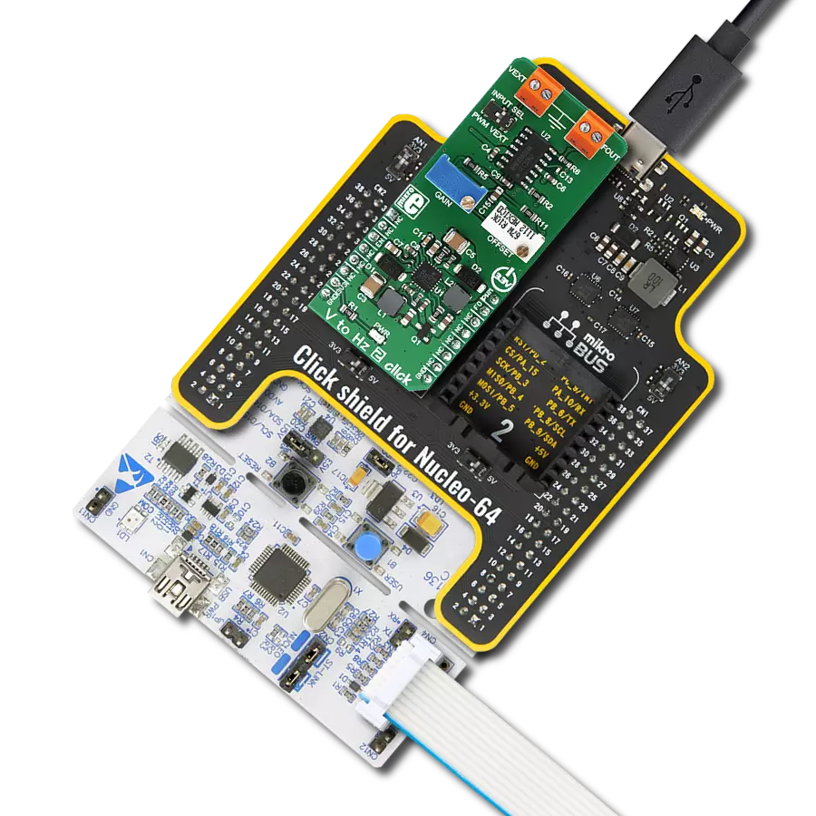
V to Hz 3 Click
Dev. board
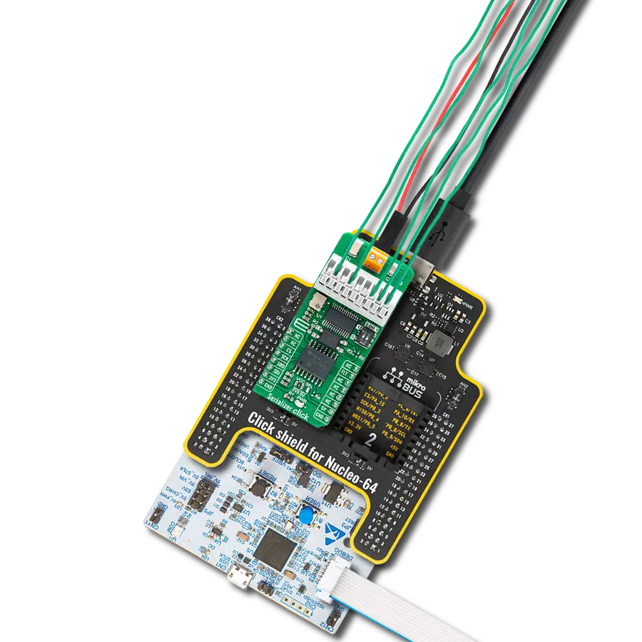
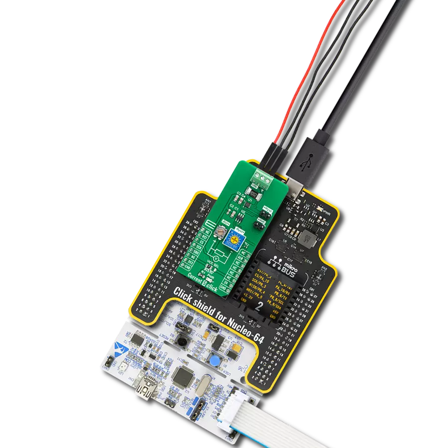
Nucleo-64 with STM32F091RC MCU
Compiler
NECTO Studio
MCU
STM32F091RC
Provides accurate output frequency proportional to its input voltage
A
A
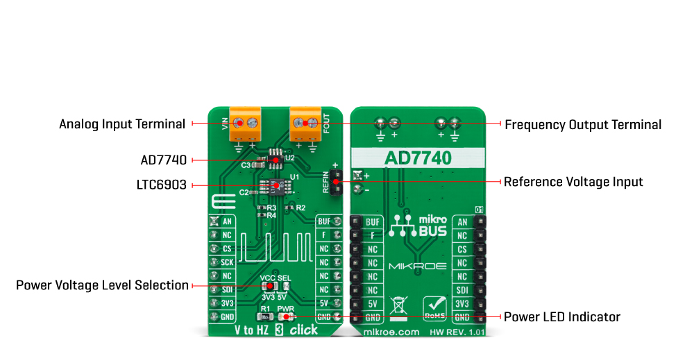
Hardware Overview
How does it work?
V to Hz 3 Click is based on the AD7740, a CMOS synchronous Voltage-to-Frequency Converter (VFC), which uses a charge-balanced conversion technique from Analog Devices. The input voltage signal from 0V up to 5V from its VIN terminal is applied to a proprietary front-end based around an analog modulator that converts the input voltage into an output pulse train. Depending on the analog input value, the output frequency goes from 10% to 90% of the input frequency provided by the SPI-configurable LTC6903 programmable oscillator, with a maximum input frequency of 1MHz. The analog input signal to the AD7740 is continuously sampled by a switched capacitor modulator whose sampling rate
is set by a master clock (primary input frequency of the AD7740). The input signal may also be buffered, setting the BUF pin of the mikroBUS™ socket to a high logic state before being applied to the sampling capacitor of the modulator, isolating the sampling capacitor charging currents from the analog input pin. The AD7740 also contains an on-chip 2.5 V default bandgap reference, the reference input to the core of the AD7740 defining the span of the VFC. Alternatively, an external reference may be used to overdrive the internal reference by applying it to an onboard header marked as REFIN. Alongside SPI communication, this Click board™ also uses several additional pins. The BUF pin mentioned above represents the
Buffered mode selection, while the AN pin indicates the presence of an external analog signal. The last of the enabled pins is the F signal, routed to the INT pin of the mikroBUS™ socket, which can also serve as output frequency from the AD7740 in the same way as the FOUT terminal. This Click board™ can operate with both 3.3V and 5V logic voltage levels selected via the VCC SEL jumper. This way, it is allowed for both 3.3V and 5V capable MCUs to use the communication lines properly. However, the Click board™ comes equipped with a library containing easy-to-use functions and an example code that can be used, as a reference, for further development.
Features overview
Development board
Nucleo-64 with STM32F091RC MCU offers a cost-effective and adaptable platform for developers to explore new ideas and prototype their designs. This board harnesses the versatility of the STM32 microcontroller, enabling users to select the optimal balance of performance and power consumption for their projects. It accommodates the STM32 microcontroller in the LQFP64 package and includes essential components such as a user LED, which doubles as an ARDUINO® signal, alongside user and reset push-buttons, and a 32.768kHz crystal oscillator for precise timing operations. Designed with expansion and flexibility in mind, the Nucleo-64 board features an ARDUINO® Uno V3 expansion connector and ST morpho extension pin
headers, granting complete access to the STM32's I/Os for comprehensive project integration. Power supply options are adaptable, supporting ST-LINK USB VBUS or external power sources, ensuring adaptability in various development environments. The board also has an on-board ST-LINK debugger/programmer with USB re-enumeration capability, simplifying the programming and debugging process. Moreover, the board is designed to simplify advanced development with its external SMPS for efficient Vcore logic supply, support for USB Device full speed or USB SNK/UFP full speed, and built-in cryptographic features, enhancing both the power efficiency and security of projects. Additional connectivity is
provided through dedicated connectors for external SMPS experimentation, a USB connector for the ST-LINK, and a MIPI® debug connector, expanding the possibilities for hardware interfacing and experimentation. Developers will find extensive support through comprehensive free software libraries and examples, courtesy of the STM32Cube MCU Package. This, combined with compatibility with a wide array of Integrated Development Environments (IDEs), including IAR Embedded Workbench®, MDK-ARM, and STM32CubeIDE, ensures a smooth and efficient development experience, allowing users to fully leverage the capabilities of the Nucleo-64 board in their projects.

Microcontroller Overview
MCU Card / MCU

Architecture
ARM Cortex-M0
MCU Memory (KB)
256
Silicon Vendor
STMicroelectronics
Pin count
64
RAM (Bytes)
32768
You complete me!
Accessories
Click Shield for Nucleo-64 comes equipped with two proprietary mikroBUS™ sockets, allowing all the Click board™ devices to be interfaced with the STM32 Nucleo-64 board with no effort. This way, Mikroe allows its users to add any functionality from our ever-growing range of Click boards™, such as WiFi, GSM, GPS, Bluetooth, ZigBee, environmental sensors, LEDs, speech recognition, motor control, movement sensors, and many more. More than 1537 Click boards™, which can be stacked and integrated, are at your disposal. The STM32 Nucleo-64 boards are based on the microcontrollers in 64-pin packages, a 32-bit MCU with an ARM Cortex M4 processor operating at 84MHz, 512Kb Flash, and 96KB SRAM, divided into two regions where the top section represents the ST-Link/V2 debugger and programmer while the bottom section of the board is an actual development board. These boards are controlled and powered conveniently through a USB connection to program and efficiently debug the Nucleo-64 board out of the box, with an additional USB cable connected to the USB mini port on the board. Most of the STM32 microcontroller pins are brought to the IO pins on the left and right edge of the board, which are then connected to two existing mikroBUS™ sockets. This Click Shield also has several switches that perform functions such as selecting the logic levels of analog signals on mikroBUS™ sockets and selecting logic voltage levels of the mikroBUS™ sockets themselves. Besides, the user is offered the possibility of using any Click board™ with the help of existing bidirectional level-shifting voltage translators, regardless of whether the Click board™ operates at a 3.3V or 5V logic voltage level. Once you connect the STM32 Nucleo-64 board with our Click Shield for Nucleo-64, you can access hundreds of Click boards™, working with 3.3V or 5V logic voltage levels.

Used MCU Pins
mikroBUS™ mapper
Take a closer look
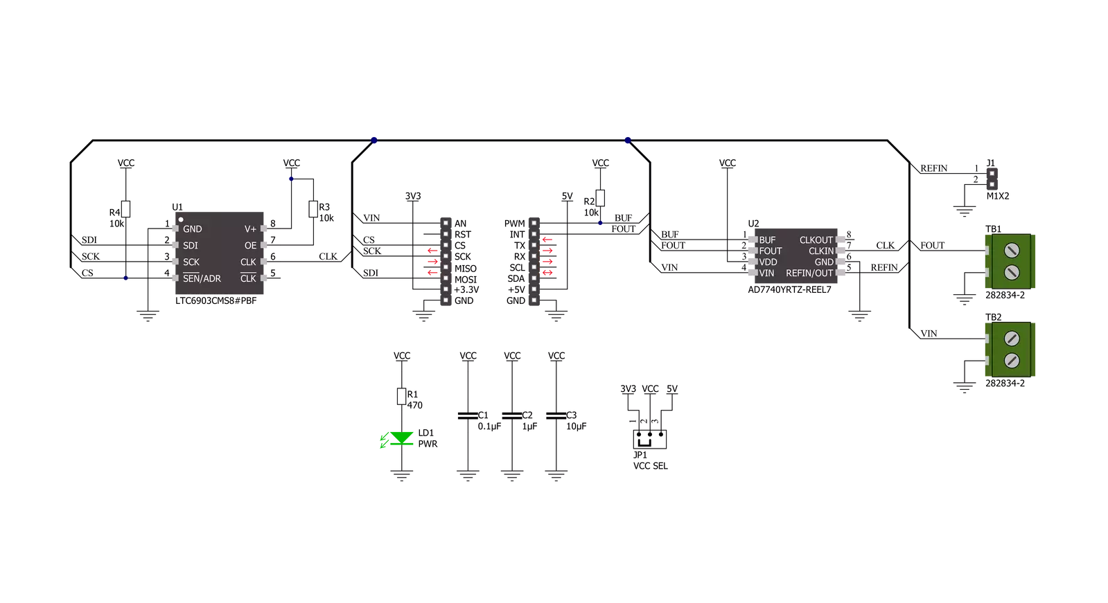
Click board™ Schematic
Step by step
Project assembly
Start by selecting your development board and Click board™. Begin with the Nucleo-64 with STM32F091RC MCU as your development board.


Software Support
Library Description
This library contains API for V to Hz 3 Click driver.
Key functions:
vtohz3_set_input_frequencyThis function enables and sets the output frequency of the programmable oscillator, which is the AD7740 input frequency.vtohz3_read_an_pin_voltageThis function reads the results of the AD conversion of the AN pin and converts them to a proportional voltage level.vtohz3_get_frequencyThis function converts voltage to the estimated output frequency in Hz.
Open Source
Code example
The complete application code and a ready-to-use project are available through the NECTO Studio Package Manager for direct installation in the NECTO Studio. The application code can also be found on the MIKROE GitHub account.
/*!
 * @file main.c
 * @brief VtoHz3 Click example
 *
 * # Description
 * This example demonstrates the use of the V to Hz 3 Click board by calculating
 * the estimated output frequency from the input voltage.
 *
 * The demo application is composed of two sections :
 *
 * ## Application Init
 * Initializes the driver and sets the input frequency.
 *
 * ## Application Task
 * Reads the input voltage from AN pin and calculates the output frequency from it.
 * The results are being displayed on the USB UART approximately once per second.
 *
 * @author Stefan Filipovic
 *
 */

#include "board.h"
#include "log.h"
#include "vtohz3.h"

static vtohz3_t vtohz3;
static log_t logger;

void application_init ( void )
{
    log_cfg_t log_cfg;        /**< Logger config object. */
    vtohz3_cfg_t vtohz3_cfg;  /**< Click config object. */

    /**
     * Logger initialization.
     * Default baud rate: 115200
     * Default log level: LOG_LEVEL_DEBUG
     * @note If USB_UART_RX and USB_UART_TX
     * are defined as HAL_PIN_NC, you will
     * need to define them manually for log to work.
     * See @b LOG_MAP_USB_UART macro definition for detailed explanation.
     */
    LOG_MAP_USB_UART( log_cfg );
    log_init( &logger, &log_cfg );
    log_info( &logger, " Application Init " );

    // Click initialization.
    vtohz3_cfg_setup( &vtohz3_cfg );
    VTOHZ3_MAP_MIKROBUS( vtohz3_cfg, MIKROBUS_1 );
    if ( SPI_MASTER_ERROR == vtohz3_init( &vtohz3, &vtohz3_cfg ) )
    {
        log_error( &logger, " Application Init Error. " );
        log_info( &logger, " Please, run program again... " );

        for ( ; ; );
    }

    vtohz3_set_input_frequency ( &vtohz3, VTOHZ3_DEFAULT_IN_FREQUENCY );
    log_info( &logger, " Application Task " );
}

void application_task ( void )
{
    float voltage;
    if ( VTOHZ3_OK == vtohz3_read_an_pin_voltage ( &vtohz3, &voltage ) )
    {
        log_printf( &logger, " Voltage : %.2f V\r\n", voltage );
        log_printf( &logger, " Output frequency : %lu Hz\r\n\n",
                    vtohz3_get_frequency ( &vtohz3, voltage, VTOHZ3_VREF_INTERNAL_2V5 ) );
    }
    Delay_ms ( 1000 );
}

int main ( void )
{
    /* Do not remove this line or clock might not be set correctly. */
    #ifdef PREINIT_SUPPORTED
    preinit();
    #endif

    application_init( );

    for ( ; ; )
    {
        application_task( );
    }

    return 0;
}

// ------------------------------------------------------------------------ END
Additional Support
Resources
Category:Measurements