Deliver the high-speed memory needed for cutting-edge applications using CY14B512Q and STM32F031K6
Your data, instantly accessible – Thanks to SRAM

Published Oct 01, 2024
Click board™
SRAM 4 Click
Dev. board
Nucleo 32 with STM32F031K6 MCU
Compiler
NECTO Studio
MCU
STM32F031K6
SRAM's combination of speed and power efficiency makes it an essential component in the world of modern electronics
A
A
Hardware Overview
How does it work?
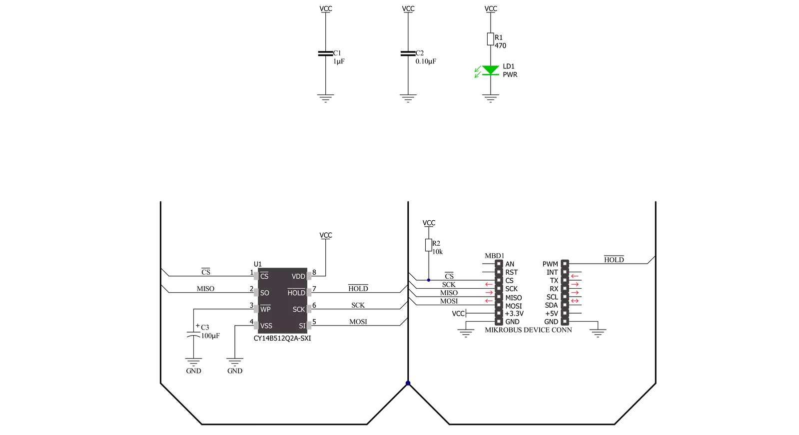
SRAM 4 Click is based on the CY14B512Q, a 512Kbit nvSRAM memory organized as 64K words of 8 bits each from Infineon. The nvSRAM specifies one million endurance cycles for nonvolatile cells with data retention of a minimum of 20 years. All the reads and writes to nvSRAM happen to the SRAM, which gives nvSRAM the unique capability to handle infinite writes to the memory. The embedded nonvolatile elements incorporate the QuantumTrap technology, making this Click board™ an ideal choice for secure data storage, creating the world’s most reliable nonvolatile memory. The CY14B512Q communicates with MCU through a standard SPI interface that enables very high clock speeds up to 40MHz with zero cycle
delay read and write cycles. It also supports the two most common modes, SPI Mode 0 and 3, and 104 MHz SPI access speed with special instructions for the read operation. Besides, the SRAM 4 Click also has an additional HOLD signal, routed to the PWM pin of the mikroBUS™ socket labeled as HLD, used to suspend the serial communication without resetting the serial sequence. The CY14B512Q uses the standard SPI opcodes for memory access. In addition to the general SPI instructions for reading and writing, also provide four special instructions: STORE, RECALL, AutoStore Disable, and AutoStore Enable. The significant benefit of this memory over serial EEPROMs is that all reads and writes to nvSRAM
are performed at the speed of the SPI bus with zero cycle delay. Therefore, no wait time is required after any of the memory accesses. Only the STORE and RECALL operations need finite time to complete, and all memory accesses are inhibited during this time. This Click board™ can be operated only with a 3.3V logic voltage level. The board must perform appropriate logic voltage level conversion before using MCUs with different logic levels. Also, it comes equipped with a library containing functions and an example code that can be used as a reference for further development.

Features overview
Development board
Nucleo 32 with STM32F031K6 MCU board provides an affordable and flexible platform for experimenting with STM32 microcontrollers in 32-pin packages. Featuring Arduino™ Nano connectivity, it allows easy expansion with specialized shields, while being mbed-enabled for seamless integration with online resources. The
board includes an on-board ST-LINK/V2-1 debugger/programmer, supporting USB reenumeration with three interfaces: Virtual Com port, mass storage, and debug port. It offers a flexible power supply through either USB VBUS or an external source. Additionally, it includes three LEDs (LD1 for USB communication, LD2 for power,
and LD3 as a user LED) and a reset push button. The STM32 Nucleo-32 board is supported by various Integrated Development Environments (IDEs) such as IAR™, Keil®, and GCC-based IDEs like AC6 SW4STM32, making it a versatile tool for developers.

Microcontroller Overview
MCU Card / MCU

Architecture
ARM Cortex-M0
MCU Memory (KB)
32
Silicon Vendor
STMicroelectronics
Pin count
32
RAM (Bytes)
4096
You complete me!
Accessories
Click Shield for Nucleo-32 is the perfect way to expand your development board's functionalities with STM32 Nucleo-32 pinout. The Click Shield for Nucleo-32 provides two mikroBUS™ sockets to add any functionality from our ever-growing range of Click boards™. We are fully stocked with everything, from sensors and WiFi transceivers to motor control and audio amplifiers. The Click Shield for Nucleo-32 is compatible with the STM32 Nucleo-32 board, providing an affordable and flexible way for users to try out new ideas and quickly create prototypes with any STM32 microcontrollers, choosing from the various combinations of performance, power consumption, and features. The STM32 Nucleo-32 boards do not require any separate probe as they integrate the ST-LINK/V2-1 debugger/programmer and come with the STM32 comprehensive software HAL library and various packaged software examples. This development platform provides users with an effortless and common way to combine the STM32 Nucleo-32 footprint compatible board with their favorite Click boards™ in their upcoming projects.

Used MCU Pins
mikroBUS™ mapper
Take a closer look
Click board™ Schematic
Step by step
Project assembly

Start by selecting your development board and Click board™. Begin with the Nucleo 32 with STM32F031K6 MCU as your development board.


Track your results in real time
Application Output
1. Application Output - In Debug mode, the 'Application Output' window enables real-time data monitoring, offering direct insight into execution results. Ensure proper data display by configuring the environment correctly using the provided tutorial.

2. UART Terminal - Use the UART Terminal to monitor data transmission via a USB to UART converter, allowing direct communication between the Click board™ and your development system. Configure the baud rate and other serial settings according to your project's requirements to ensure proper functionality. For step-by-step setup instructions, refer to the provided tutorial.

3. Plot Output - The Plot feature offers a powerful way to visualize real-time sensor data, enabling trend analysis, debugging, and comparison of multiple data points. To set it up correctly, follow the provided tutorial, which includes a step-by-step example of using the Plot feature to display Click board™ readings. To use the Plot feature in your code, use the function: plot(*insert_graph_name*, variable_name);. This is a general format, and it is up to the user to replace 'insert_graph_name' with the actual graph name and 'variable_name' with the parameter to be displayed.

Software Support
Library Description
This library contains API for SRAM 4 Click driver.
Key functions:
sram4_memory_read- Read data from memory.sram4_memory_write- Write data to memory.sram4_generic_command- Command writing function.
Open Source
Code example
The complete application code and a ready-to-use project are available through the NECTO Studio Package Manager for direct installation in the NECTO Studio. The application code can also be found on the MIKROE GitHub account.
/*!
 * @file main.c
 * @brief SRAM4 Click example
 *
 * # Description
 * This example application showcases ability of device
 * ability to manipulate with memory( writing and reading data ).
 *
 * The demo application is composed of two sections :
 *
 * ## Application Init
 * Initialization of communication modules(SPI, UART) and additional
 * pins. Reads ID and checks if it matches with SRAM4_DEVICE_ID to
 * check communication. Then clears protection from memory access.
 *
 * ## Application Task
 * Writes 3 times to memory with length of data offset in memory address.
 * Then reads 2 times first 2 data written should be read in one read,
 * and 3rd write should be read separately.
 *
 * @author Luka FIlipovic
 *
 */

#include "board.h"
#include "log.h"
#include "sram4.h"

static sram4_t sram4;
static log_t logger;

void application_init ( void )
{
    log_cfg_t log_cfg;  /**< Logger config object. */
    sram4_cfg_t sram4_cfg;  /**< Click config object. */

    /**
     * Logger initialization.
     * Default baud rate: 115200
     * Default log level: LOG_LEVEL_DEBUG
     * @note If USB_UART_RX and USB_UART_TX
     * are defined as HAL_PIN_NC, you will
     * need to define them manually for log to work.
     * See @b LOG_MAP_USB_UART macro definition for detailed explanation.
     */
    LOG_MAP_USB_UART( log_cfg );
    log_init( &logger, &log_cfg );
    log_info( &logger, " Application Init " );

    // Click initialization.
    sram4_cfg_setup( &sram4_cfg );
    SRAM4_MAP_MIKROBUS( sram4_cfg, MIKROBUS_1 );
    err_t init_flag  = sram4_init( &sram4, &sram4_cfg );
    if ( SPI_MASTER_ERROR == init_flag )
    {
        log_error( &logger, " Application Init Error. " );
        log_info( &logger, " Please, run program again... " );
        for ( ; ; );
    }

    if ( sram4_default_cfg ( &sram4 ) )
    {
        log_error( &logger, " Default configuration. " );
        log_info( &logger, " Please, run program again... " );
        for ( ; ; );
    }

    log_info( &logger, " Application Task " );
}

void application_task ( void )
{
    char read_buf[ 100 ] = { 0 };
    char click_name[ ] = "SRAM 4";
    char company_name[ ] = "MikroE";
    char product_name[ ] = " Click board";
    static const uint16_t START_ADR = 0x0001;
    uint16_t mem_adr = START_ADR;

    //Write Data
    sram4_memory_write( &sram4, mem_adr, click_name, strlen( click_name ) );
    mem_adr += strlen( click_name );
    sram4_memory_write( &sram4, mem_adr, product_name, strlen( product_name ) );
    mem_adr += strlen( product_name );
    sram4_memory_write( &sram4, mem_adr, company_name, strlen( company_name ) );

    //Read Data
    mem_adr = START_ADR;
    sram4_memory_read( &sram4, mem_adr, read_buf, strlen( click_name ) + strlen( product_name ) );
    log_printf( &logger, " > Read Data from 0x%.4X memory address: %s\r\n", mem_adr, read_buf );
    memset( read_buf, 0, strlen( read_buf ) );
    mem_adr += strlen(click_name) + strlen( product_name );
    sram4_memory_read( &sram4, mem_adr, read_buf, strlen( company_name ) );
    log_printf( &logger, " > Read Data from 0x%.4X memory address: %s\r\n", mem_adr, read_buf );
    log_printf( &logger, "**********************************************************************\r\n" );

    Delay_ms( 3000 );
}

void main ( void )
{
    application_init( );

    for ( ; ; )
    {
        application_task( );
    }
}

// ------------------------------------------------------------------------ END


