Hear what your heart speaks with VEMD8080 and STM32G474RE
BeatTrack

Published Nov 08, 2024
Click board™
Heart Rate 7 Click
Dev. board
Nucleo 64 with STM32G474RE MCU
Compiler
NECTO Studio
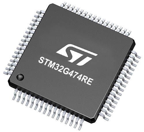
MCU
STM32G474RE
Provide real-time and accurate measurements of your heart's beats per minute that help you to track and manage your cardiovascular health
A
A
Hardware Overview
How does it work?
Heart Rate 7 Click is based on the VEMD8080 photo-sensor from Vishay, a high-speed PD element with enhanced sensitivity in the visible light spectrum. The Click board™ also uses two VLMTG1400, high-brightness true-green LEDs from Vishay, specially designed for the HRM measurement applications, offering a narrow band of green light wavelength. Heart Rate 7 click consists of an analog front end and the optical front end. The main task of the analog front-end IC is to drive LEDs and condition the signal received by the photo-diode (PD) by eliminating the background noise and ambient light influence. Besides that, it also provides conversion of the measurement into digital information, which an MCU can use. For the conversion to be accurate, the analog front-end device must not introduce any artifacts into the readings. Heart Rate 7 Click employs AFE4404, an integrated analog front-end (AFE) device used for optical heart-rate monitoring and bio-sensing from Texas Instruments to achieve accurate measurements. This IC supports up to three switching LEDs and a single PD element. The current from the PD element is converted to a linear voltage by means of the integrated trans-impedance amplifier section (TIA) with a programmable gain so that it can be sampled by the AD section, which features a 22-bit ADC converter. The signal chain is kept fully differential throughout the receiver channel to achieve good rejection of common-mode noise and the noise from the power supply. The AFE IC uses the I2C communication, with its pins routed to the corresponding mikroBUS™ I2C pins.
The analog front-end IC works with periodically repeated operations (a pulse repetition frequency or PRF). There are four sampling phases per cycle. The four different readings are stored in separate 24-bit output registers. There are also four filters on the TIA output, which allow pulses from the PD to pass through the ADC, isolating the time when the emitting LEDs are ON and switching to the different filters in every sampling phase. The sampling phases are determined by the LED modes: two LED modes or three LED modes. This affects which LEDs are pulsed during the corresponding sampling cycles – LED1 and LED2, or LED 1, LED 2, and LED 3. However, the Heart Rate 7 click features only 2 LEDs, so the three LED modes should not be used. The analog front-end AFE4404 IC also incorporates a DAC to cancel the DC offset from the PD. When the TIA gain is set to a high value, it will amplify the DC component of the PD signal, too. This DC component needs to be removed from the signal path to allow proper ADC conversion, so the DAC that sources current in the opposite direction with respect to the existing DC offset is employed at the input stage. This allows for higher amplification of the signal from the PD and, thus, more useful (AC) signal detection sensitivity. LED drivers individually allow 6 bits of LED current control for each channel. This allows 63 steps between 0 and 50mA. This range can be doubled to 100mA. The onboard SMD jumper, labeled as the LED SUP, can set the LED driver supply voltage. It offers a selection between 3.3V and 5V. The ADC_RDY pin provides an interrupt to the host MCU, saving it from having to poll the
sensor for data constantly. This pin is set to a HIGH logic level when the PRF cycle ends, allowing four output data register to be read. The PRF can vary between 10 to 1000 samples per second. This pin is routed to the INT pin of the mikroBUS™. The AFE4404 IC can be clocked both internally and externally. It is advised to drive the Heart Rate 7 Click by the same clock as the host MCU for a precise and synchronized measurement. The input clock can go up to 60MHz, but the internal divider of the IC has to be set so that the clock stays within the range from 4MHz to 6MHz. When driven by the internal clock, the device runs at 4MHz. By default, the external clock input is selected. The clock signal can be introduced via the PWM pin of the mikroBUS™. After the power-on, the AFE IC requires a reset. The RESETZ pin of this IC is routed to the RST pin of the mikroBUS™, allowing it to be reset by the host MCU. Pulling this signal to a LOW logic level of about 25 µs to 50 µs will cause a device reset. Pulling this pin for more than 200 µs will put the device into the Power Down mode. The device can also be reset by setting a bit in the appropriate register via the I2C. The onboard pull-up resistor pulls This pin to a HIGH logic level. More information about the registers and how to set them can be found in the AFE4404 IC datasheet. However, included library contains functions that allow easy configuration and use of the Heart Rate 7 click. The included example (demo) application demonstrates its functionality and can be used as a reference for a custom design.


Features overview
Development board
Nucleo-64 with STM32G474R MCU offers a cost-effective and adaptable platform for developers to explore new ideas and prototype their designs. This board harnesses the versatility of the STM32 microcontroller, enabling users to select the optimal balance of performance and power consumption for their projects. It accommodates the STM32 microcontroller in the LQFP64 package and includes essential components such as a user LED, which doubles as an ARDUINO® signal, alongside user and reset push-buttons, and a 32.768kHz crystal oscillator for precise timing operations. Designed with expansion and flexibility in mind, the Nucleo-64 board features an ARDUINO® Uno V3 expansion connector and ST morpho extension pin
headers, granting complete access to the STM32's I/Os for comprehensive project integration. Power supply options are adaptable, supporting ST-LINK USB VBUS or external power sources, ensuring adaptability in various development environments. The board also has an on-board ST-LINK debugger/programmer with USB re-enumeration capability, simplifying the programming and debugging process. Moreover, the board is designed to simplify advanced development with its external SMPS for efficient Vcore logic supply, support for USB Device full speed or USB SNK/UFP full speed, and built-in cryptographic features, enhancing both the power efficiency and security of projects. Additional connectivity is
provided through dedicated connectors for external SMPS experimentation, a USB connector for the ST-LINK, and a MIPI® debug connector, expanding the possibilities for hardware interfacing and experimentation. Developers will find extensive support through comprehensive free software libraries and examples, courtesy of the STM32Cube MCU Package. This, combined with compatibility with a wide array of Integrated Development Environments (IDEs), including IAR Embedded Workbench®, MDK-ARM, and STM32CubeIDE, ensures a smooth and efficient development experience, allowing users to fully leverage the capabilities of the Nucleo-64 board in their projects.

Microcontroller Overview
MCU Card / MCU
Architecture
ARM Cortex-M4
MCU Memory (KB)
512
Silicon Vendor
STMicroelectronics
Pin count
64
RAM (Bytes)
128k
You complete me!
Accessories
Click Shield for Nucleo-64 comes equipped with two proprietary mikroBUS™ sockets, allowing all the Click board™ devices to be interfaced with the STM32 Nucleo-64 board with no effort. This way, Mikroe allows its users to add any functionality from our ever-growing range of Click boards™, such as WiFi, GSM, GPS, Bluetooth, ZigBee, environmental sensors, LEDs, speech recognition, motor control, movement sensors, and many more. More than 1537 Click boards™, which can be stacked and integrated, are at your disposal. The STM32 Nucleo-64 boards are based on the microcontrollers in 64-pin packages, a 32-bit MCU with an ARM Cortex M4 processor operating at 84MHz, 512Kb Flash, and 96KB SRAM, divided into two regions where the top section represents the ST-Link/V2 debugger and programmer while the bottom section of the board is an actual development board. These boards are controlled and powered conveniently through a USB connection to program and efficiently debug the Nucleo-64 board out of the box, with an additional USB cable connected to the USB mini port on the board. Most of the STM32 microcontroller pins are brought to the IO pins on the left and right edge of the board, which are then connected to two existing mikroBUS™ sockets. This Click Shield also has several switches that perform functions such as selecting the logic levels of analog signals on mikroBUS™ sockets and selecting logic voltage levels of the mikroBUS™ sockets themselves. Besides, the user is offered the possibility of using any Click board™ with the help of existing bidirectional level-shifting voltage translators, regardless of whether the Click board™ operates at a 3.3V or 5V logic voltage level. Once you connect the STM32 Nucleo-64 board with our Click Shield for Nucleo-64, you can access hundreds of Click boards™, working with 3.3V or 5V logic voltage levels.

Used MCU Pins
mikroBUS™ mapper
Take a closer look
Click board™ Schematic

Step by step
Project assembly
Start by selecting your development board and Click board™. Begin with the Nucleo 64 with STM32G474RE MCU as your development board.


Track your results in real time
Application Output
1. Application Output - In Debug mode, the 'Application Output' window enables real-time data monitoring, offering direct insight into execution results. Ensure proper data display by configuring the environment correctly using the provided tutorial.

2. UART Terminal - Use the UART Terminal to monitor data transmission via a USB to UART converter, allowing direct communication between the Click board™ and your development system. Configure the baud rate and other serial settings according to your project's requirements to ensure proper functionality. For step-by-step setup instructions, refer to the provided tutorial.

3. Plot Output - The Plot feature offers a powerful way to visualize real-time sensor data, enabling trend analysis, debugging, and comparison of multiple data points. To set it up correctly, follow the provided tutorial, which includes a step-by-step example of using the Plot feature to display Click board™ readings. To use the Plot feature in your code, use the function: plot(*insert_graph_name*, variable_name);. This is a general format, and it is up to the user to replace 'insert_graph_name' with the actual graph name and 'variable_name' with the parameter to be displayed.

Software Support
Library Description
This library contains API for Heart rate 7 Click driver.
Key functions:
heartrate7_write_reg- Heart Rate 7 register write functionheartrate7_read_reg- Heart Rate 7 register reading functionheartrate7_sw_reset- Heart Rate 7 software reset function
Open Source
Code example
The complete application code and a ready-to-use project are available through the NECTO Studio Package Manager for direct installation in the NECTO Studio. The application code can also be found on the MIKROE GitHub account.
/*!
 * @file main.c
 * @brief HeartRate7 Click example
 *
 * # Description
 * This example showcases ability for device to read Heart Rate 7 Click Board.
 *
 * The demo application is composed of two sections :
 *
 * ## Application Init
 * Configures the micro controller for communication and initializes the click board.
 *
 * ## Application Task
 * This section shows how the data is processed and sent to the MikroPlot application.
 *
 * @note For testing this example application SerialPlot was used.
 * There you can see heart rate graphicly shown.
 *
 * @author Stefan Ilic
 *
 */

#include "board.h"
#include "log.h"
#include "heartrate7.h"

static heartrate7_t heartrate7;
static log_t logger;
static uint32_t sensor_value;
static uint32_t time = 0;

void application_init ( void )
{
    log_cfg_t log_cfg;  /**< Logger config object. */
    heartrate7_cfg_t heartrate7_cfg;  /**< Click config object. */

    /**
     * Logger initialization.
     * Default baud rate: 115200
     * Default log level: LOG_LEVEL_DEBUG
     * @note If USB_UART_RX and USB_UART_TX
     * are defined as HAL_PIN_NC, you will
     * need to define them manually for log to work.
     * See @b LOG_MAP_USB_UART macro definition for detailed explanation.
     */
    LOG_MAP_USB_UART( log_cfg );
    log_init( &logger, &log_cfg );
    log_info( &logger, " Application Init " );

    // Click initialization.
    heartrate7_cfg_setup( &heartrate7_cfg );
    HEARTRATE7_MAP_MIKROBUS( heartrate7_cfg, MIKROBUS_1 );
    if ( I2C_MASTER_ERROR == heartrate7_init( &heartrate7, &heartrate7_cfg ) )
    {
        log_error( &logger, " Communication init." );
        for ( ; ; );
    }

    if ( HEARTRATE7_ERROR == heartrate7_default_cfg ( &heartrate7 ) )
    {
        log_error( &logger, " Default configuration." );
        for ( ; ; );
    }

    log_info( &logger, " Application Task " );
}

void application_task ( void )
{
    sensor_value = heartrate7_get_aled1_val( &heartrate7 );
    log_printf( &logger, "%lu,%lu \r\n", sensor_value, time );
    time += 10;
    Delay_ms( 10 );
}

void main ( void )
{
    application_init( );

    for ( ; ; )
    {
        application_task( );
    }
}

// ------------------------------------------------------------------------ END


