Experience lightning-fast data storage with the BY25Q16E and PIC32MZ2048EFM100
16Mbit SPI NOR Flash memory solution for reliable data storage

Published Apr 09, 2025
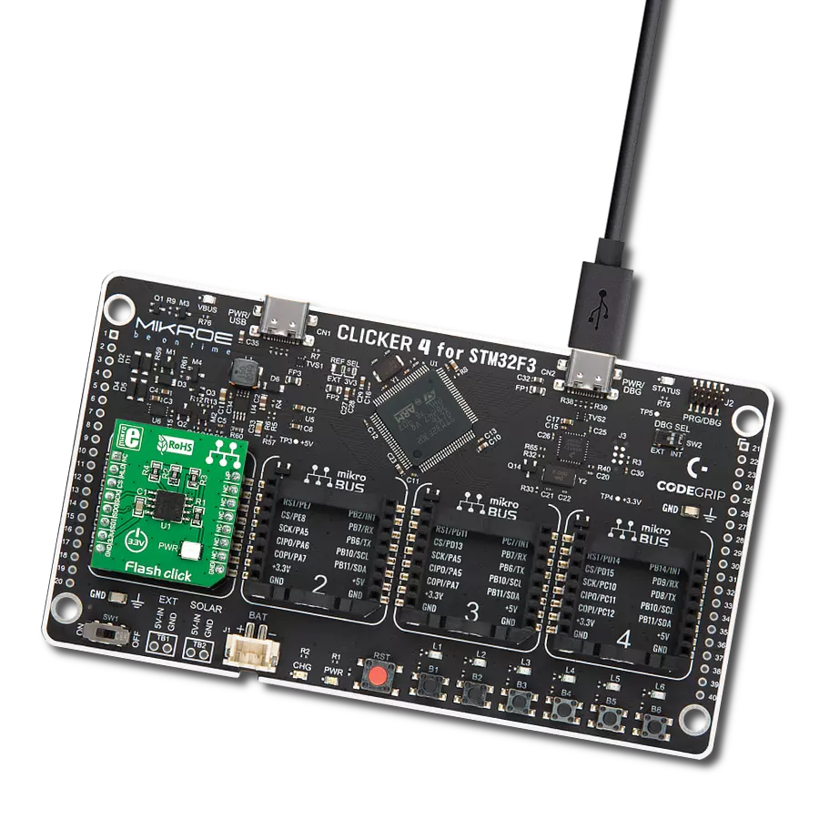
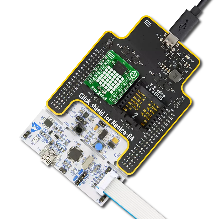
Click board™
Flash 13 Click
Dev. board
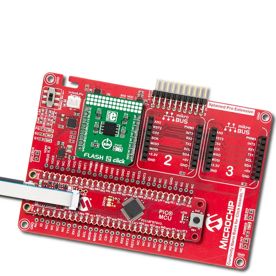
Curiosity PIC32 MZ EF
Compiler
NECTO Studio
MCU
PIC32MZ2048EFM100
Add fast, reliable, and secure SPI Flash storage to embedded apps for high-speed data retention and execution-in-place capability
A
A
Hardware Overview
How does it work?
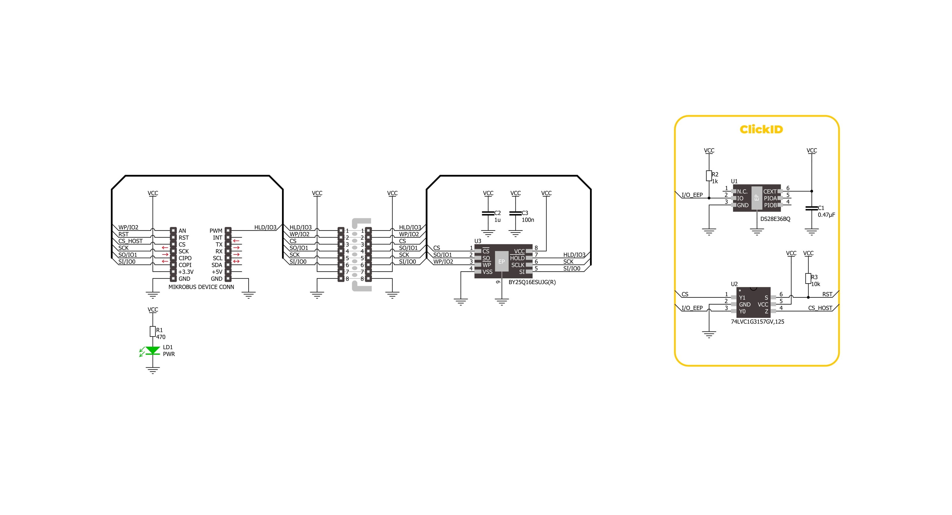
Flash 13 Click is based on the BY25Q16E, a 16Mbit SPI NOR Flash memory from BYTe Semiconductor. This memory supports a range of communication modes including standard SPI, Dual/Quad I/O SPI, and a 2-clock instruction cycle Quad Peripheral Interface (QPI), offering flexibility for embedded applications. With SPI clock frequencies reaching up to 108MHz, the BY25Q16E can achieve data transfer rates of up to 216MHz in Dual I/O mode and an impressive 432MHz in Quad I/O mode when utilizing Fast Read or QPI instructions. These high-speed operations enable performance levels that surpass those of traditional asynchronous 8-bit and 16-bit parallel flash memories, making it suitable for demanding commercial and industrial use cases that demand fast access, secure storage, and extended operational lifetime. The BY25Q16E offers high endurance with a typical lifespan of 100,000 program-erase cycles per sector and long-term reliability with a typical data retention period of 20 years. One of the standout features of the BY25Q16E is its Continuous Read Mode, which enables quick memory access by requiring just 8
clock cycles to read a 24-bit address. This capability makes true XIP (execute in place) operations possible, significantly optimizing system performance where direct code execution from Flash is required. The device also adheres to JEDEC standards by supporting standard manufacturer and device ID protocols, and it incorporates three security registers of 1024 bytes each for data protection and secure storage requirements. This Click board™ is designed in a unique format supporting the newly introduced MIKROE feature called "Click Snap." Unlike the standardized version of Click boards, this feature allows the main chip area to become movable by breaking the PCB, opening up many new possibilities for implementation. Thanks to the Snap feature, the BY25Q16E can operate autonomously by accessing their signals directly on the pins marked 1-8. Additionally, the Snap part includes a specified and fixed screw hole position, enabling users to secure the Snap board in their desired location. Flash 13 Click communicates with MCU through a standard SPI interface supporting the two most common SPI modes, SPI Mode 0 and 3, and
a maximum clock frequency of up to 108MHz. The BY25Q16E enhances data transfer rates through Dual and Quad SPI operations, which double and quadruple the standard SPI speed, respectively. These enhanced speeds are achieved by re-purposing the available pins as bidirectional I/O pins during Dual and Quad SPI operations. Furthermore, the board features a HOLD function, marked as HLD and routed on the default position of the PWM pin of the mikroBUS™ socket. The hold function allows the suspension of serial communications without disrupting ongoing operations. The board also has a Write Protect feature, marked as WP and routed on the default position of the AN of the mikroBUS™ socket, that safeguards all registers and memory from unintended write operations through both hardware and software mechanisms. This Click board™ can be operated only with a 3.3V logic voltage level. The board must perform appropriate logic voltage level conversion before using MCUs with different logic levels. It also comes equipped with a library containing functions and example code that can be used as a reference for further development.

Features overview
Development board
Curiosity PIC32 MZ EF development board is a fully integrated 32-bit development platform featuring the high-performance PIC32MZ EF Series (PIC32MZ2048EFM) that has a 2MB Flash, 512KB RAM, integrated FPU, Crypto accelerator, and excellent connectivity options. It includes an integrated programmer and debugger, requiring no additional hardware. Users can expand
functionality through MIKROE mikroBUS™ Click™ adapter boards, add Ethernet connectivity with the Microchip PHY daughter board, add WiFi connectivity capability using the Microchip expansions boards, and add audio input and output capability with Microchip audio daughter boards. These boards are fully integrated into PIC32’s powerful software framework, MPLAB Harmony,
which provides a flexible and modular interface to application development a rich set of inter-operable software stacks (TCP-IP, USB), and easy-to-use features. The Curiosity PIC32 MZ EF development board offers expansion capabilities making it an excellent choice for a rapid prototyping board in Connectivity, IOT, and general-purpose applications.

Microcontroller Overview
MCU Card / MCU
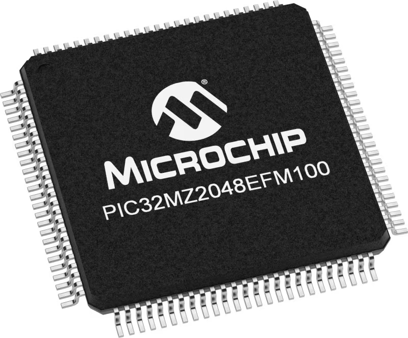
Architecture
PIC32
MCU Memory (KB)
2048
Silicon Vendor
Microchip
Pin count
100
RAM (Bytes)
524288
Used MCU Pins
mikroBUS™ mapper
Take a closer look
Click board™ Schematic
Step by step
Project assembly

Start by selecting your development board and Click board™. Begin with the Curiosity PIC32 MZ EF as your development board.


Track your results in real time
Application Output
1. Application Output - In Debug mode, the 'Application Output' window enables real-time data monitoring, offering direct insight into execution results. Ensure proper data display by configuring the environment correctly using the provided tutorial.

2. UART Terminal - Use the UART Terminal to monitor data transmission via a USB to UART converter, allowing direct communication between the Click board™ and your development system. Configure the baud rate and other serial settings according to your project's requirements to ensure proper functionality. For step-by-step setup instructions, refer to the provided tutorial.

3. Plot Output - The Plot feature offers a powerful way to visualize real-time sensor data, enabling trend analysis, debugging, and comparison of multiple data points. To set it up correctly, follow the provided tutorial, which includes a step-by-step example of using the Plot feature to display Click board™ readings. To use the Plot feature in your code, use the function: plot(*insert_graph_name*, variable_name);. This is a general format, and it is up to the user to replace 'insert_graph_name' with the actual graph name and 'variable_name' with the parameter to be displayed.

Software Support
Library Description
Flash 13 Click demo application is developed using the NECTO Studio, ensuring compatibility with mikroSDK's open-source libraries and tools. Designed for plug-and-play implementation and testing, the demo is fully compatible with all development, starter, and mikromedia boards featuring a mikroBUS™ socket.
Example Description
This example demonstrates the use of Flash 13 Click board by writing specified data to the memory and reading it back.
Key functions:
flash13_cfg_setup- This function initializes Click configuration structure to initial values.flash13_init- This function initializes all necessary pins and peripherals used for this Click board.flash13_erase_memory- This function erases the selected amount of memory which contains the selected address.flash13_memory_write- This function writes a desired number of data bytes starting from the selected memory address.flash13_memory_read- This function reads a desired number of data bytes starting from the selected memory address.
Application Init
Initializes the driver and checks the communication by reading and verifying the device ID.
Application Task
Writes a desired number of bytes to the memory and then verifies if it is written correctly by reading from the same memory location and displaying the memory content on the USB UART. The whole 4KB sector of memory that contains the STARTING_ADDRESS will be erased before writing data.
Open Source
Code example
The complete application code and a ready-to-use project are available through the NECTO Studio Package Manager for direct installation in the NECTO Studio. The application code can also be found on the MIKROE GitHub account.
/*!
 * @file main.c
 * @brief Flash 13 Click example
 *
 * # Description
 * This example demonstrates the use of Flash 13 Click board by writing specified data to
 * the memory and reading it back.
 *
 * The demo application is composed of two sections :
 *
 * ## Application Init
 * Initializes the driver and checks the communication by reading and verifying the device ID.
 *
 * ## Application Task
 * Writes a desired number of bytes to the memory and then verifies if it is written correctly
 * by reading from the same memory location and displaying the memory content on the USB UART.
 * The whole 4KB sector of memory that contains the STARTING_ADDRESS will be erased before writing data.
 *
 * @author Stefan Filipovic
 *
 */

#include "board.h"
#include "log.h"
#include "flash13.h"

#define DEMO_TEXT_MESSAGE_1         "MIKROE"
#define DEMO_TEXT_MESSAGE_2         "Flash 13 Click"
#define STARTING_ADDRESS            0x012345ul

static flash13_t flash13;
static log_t logger;

void application_init ( void )
{
    log_cfg_t log_cfg;  /**< Logger config object. */
    flash13_cfg_t flash13_cfg;  /**< Click config object. */

    /**
     * Logger initialization.
     * Default baud rate: 115200
     * Default log level: LOG_LEVEL_DEBUG
     * @note If USB_UART_RX and USB_UART_TX
     * are defined as HAL_PIN_NC, you will
     * need to define them manually for log to work.
     * See @b LOG_MAP_USB_UART macro definition for detailed explanation.
     */
    LOG_MAP_USB_UART( log_cfg );
    log_init( &logger, &log_cfg );
    log_info( &logger, " Application Init " );

    // Click initialization.
    flash13_cfg_setup( &flash13_cfg );
    FLASH13_MAP_MIKROBUS( flash13_cfg, MIKROBUS_1 );
    if ( SPI_MASTER_ERROR == flash13_init( &flash13, &flash13_cfg ) )
    {
        log_error( &logger, " Communication init." );
        for ( ; ; );
    }

    if ( FLASH13_ERROR == flash13_check_communication ( &flash13 ) )
    {
        log_error( &logger, " Check communication." );
        for ( ; ; );
    }

    log_info( &logger, " Application Task " );
}

void application_task ( void )
{
    uint8_t data_buf[ 128 ] = { 0 };

    log_printf ( &logger, " Memory address: 0x%.6LX\r\n", ( uint32_t ) STARTING_ADDRESS );
    if ( FLASH13_OK == flash13_erase_memory ( &flash13, FLASH13_CMD_SECTOR_ERASE_4KB, STARTING_ADDRESS ) )
    {
        log_printf ( &logger, " Erase memory block (4KB)\r\n" );
    }
    memcpy ( data_buf, DEMO_TEXT_MESSAGE_1, strlen ( DEMO_TEXT_MESSAGE_1 ) );
    if ( FLASH13_OK == flash13_memory_write ( &flash13, STARTING_ADDRESS, data_buf, sizeof ( data_buf ) ) )
    {
        log_printf ( &logger, " Write data: %s\r\n", data_buf );
        Delay_ms ( 100 );
    }
    memset ( data_buf, 0, sizeof ( data_buf ) );
    if ( FLASH13_OK == flash13_memory_read ( &flash13, STARTING_ADDRESS, data_buf, sizeof ( data_buf ) ) )
    {
        log_printf ( &logger, " Read data: %s\r\n\n", data_buf );
        Delay_ms ( 1000 );
        Delay_ms ( 1000 );
        Delay_ms ( 1000 );
    }

    log_printf ( &logger, " Memory address: 0x%.6LX\r\n", ( uint32_t ) STARTING_ADDRESS );
    if ( FLASH13_OK == flash13_erase_memory ( &flash13, FLASH13_CMD_SECTOR_ERASE_4KB, STARTING_ADDRESS ) )
    {
        log_printf ( &logger, " Erase memory block (4KB)\r\n" );
    }
    memcpy ( data_buf, DEMO_TEXT_MESSAGE_2, strlen ( DEMO_TEXT_MESSAGE_2 ) );
    if ( FLASH13_OK == flash13_memory_write ( &flash13, STARTING_ADDRESS, data_buf, sizeof ( data_buf ) ) )
    {
        log_printf ( &logger, " Write data: %s\r\n", data_buf );
        Delay_ms ( 100 );
    }
    memset ( data_buf, 0, sizeof ( data_buf ) );
    if ( FLASH13_OK == flash13_memory_read ( &flash13, STARTING_ADDRESS, data_buf, sizeof ( data_buf ) ) )
    {
        log_printf ( &logger, " Read data: %s\r\n\n", data_buf );
        Delay_ms ( 1000 );
        Delay_ms ( 1000 );
        Delay_ms ( 1000 );
    }
}

int main ( void )
{
    /* Do not remove this line or clock might not be set correctly. */
    #ifdef PREINIT_SUPPORTED
    preinit();
    #endif

    application_init( );

    for ( ; ; )
    {
        application_task( );
    }

    return 0;
}

// ------------------------------------------------------------------------ END
Additional Support
Resources
Category:FLASH