Achieve unparalleled switching control and reliability with AH1389 and PIC32MX675F512L
Switch with magnetism: Upgrade your control with Hall switch

Published Sep 13, 2023
Click board™
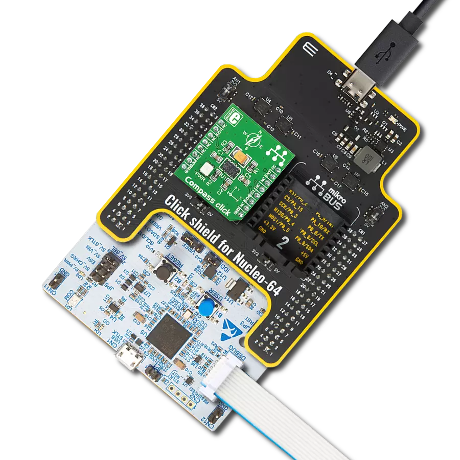
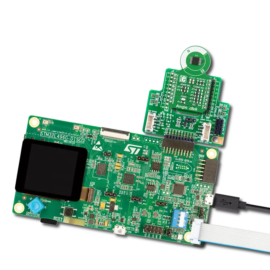
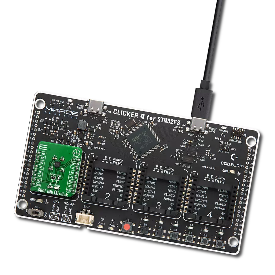
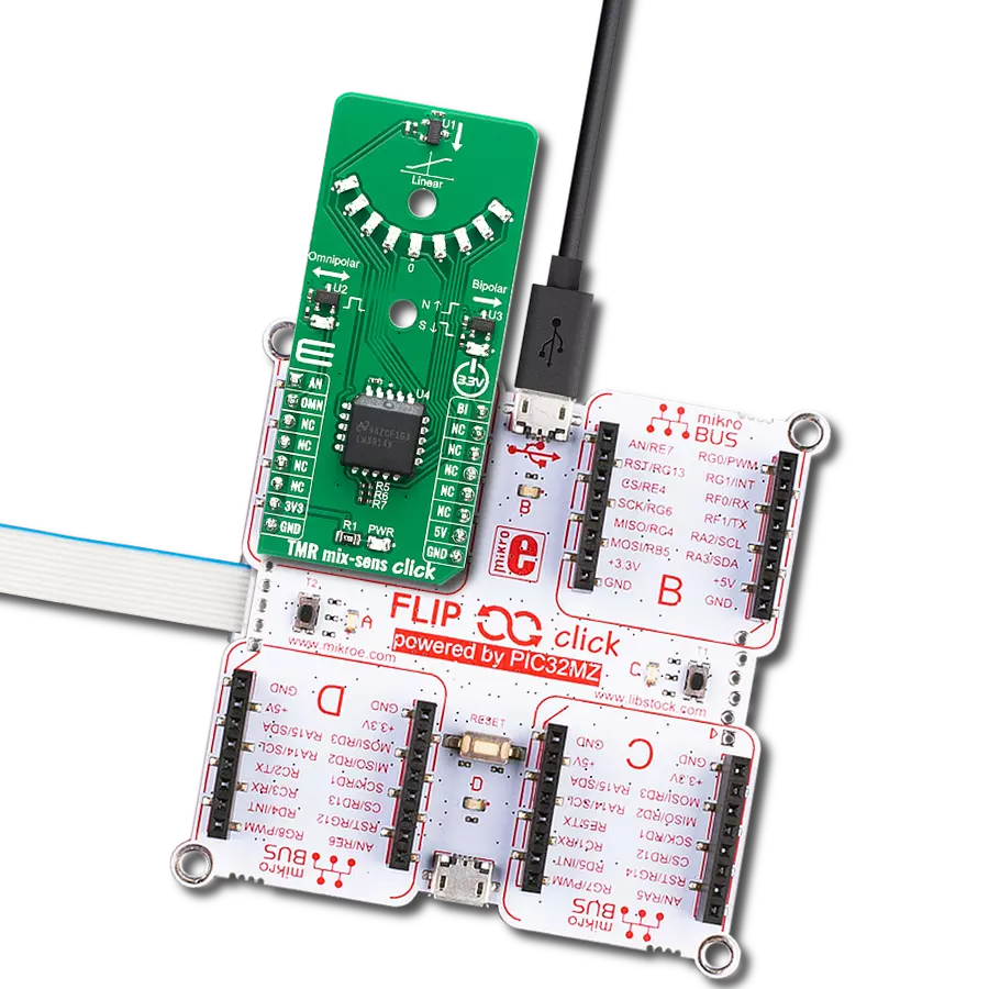
Hall Switch Click
Dev. board
UNI-DS v8
Compiler
NECTO Studio
MCU
PIC32MX675F512L
Provide precise and dependable relay control activated by magnetic fields. It empowers you to optimize applications in security systems and industrial automation with ease.
A
A
Hardware Overview
How does it work?
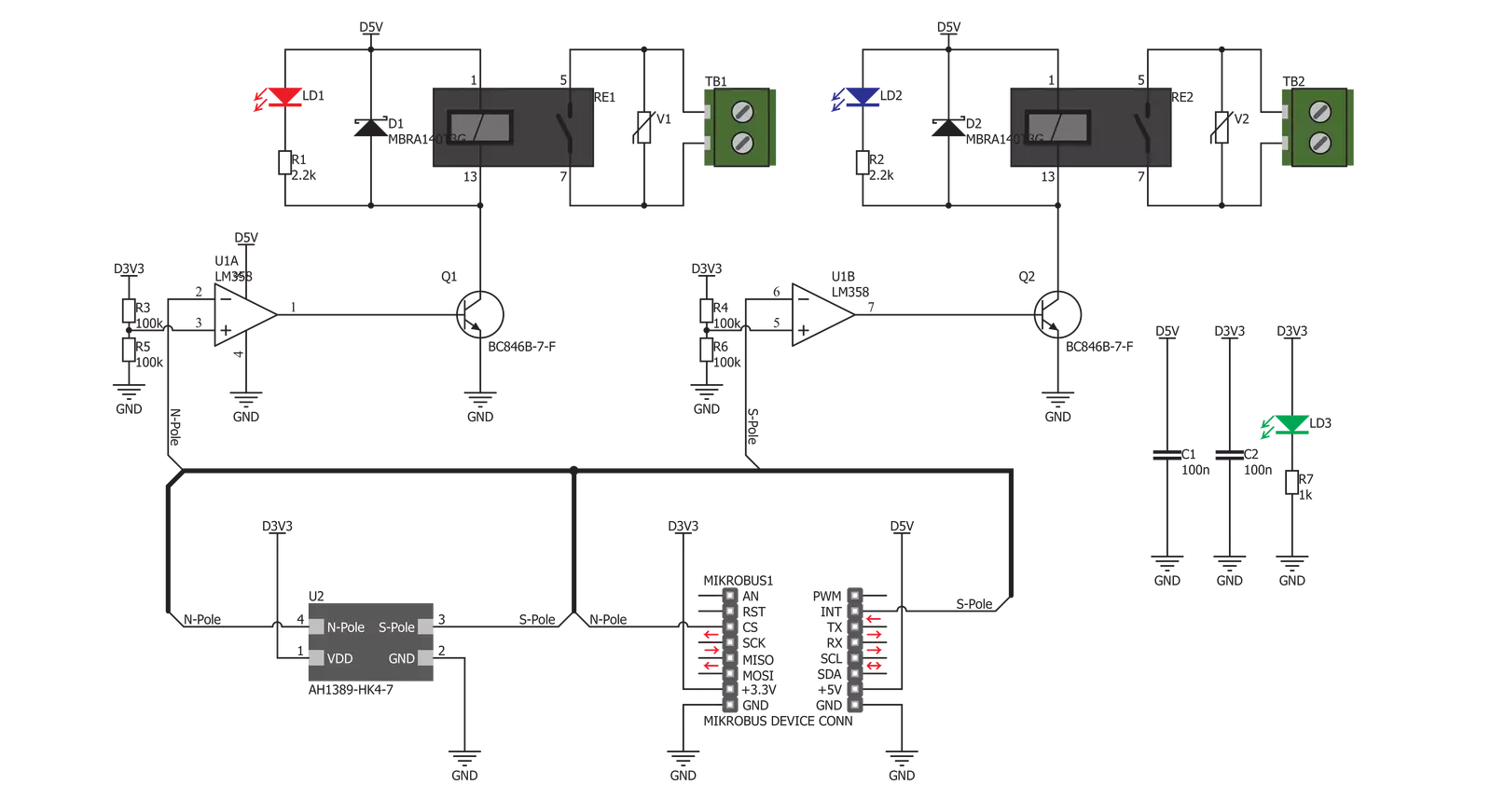
Hall Switch Click is based on the AH1389, an ultra-sensitive dual output unipolar Hall Effect switch, from Diodes Incorporated. This IC utilizes Hall effect - a phenomenon in which the current flow, or rather - the path of the conductor electrons is affected by the magnetic field. Due to the fact that the path of the electrons is curved, a buildup of positive charges is formed on the opposite side of this path, and the voltage is generated. If a voltmeter is connected to the path perpendicular to the current path and the magnetic field, a voltage will be detected. The AH1389 has the ability to detect both the north and south poles of the magnetic field. The magnetic field from the south pole magnet will pull the output 2 to a LOW (active) state, while the magnetic field from the north pole magnet will pull the output 1 to a LOW
(active) state. The IC features several sections for the signal conditioning. It also provides the hysteresis for the output activation, to avoid erratic triggering. The magnetic field strength which activates outputs is about ±25 G, while the field strength under ±20 G will deactivate outputs, giving a hysteresis of typical 5 G. The positive and negative sign is used with respect to the magnet poles (north pole has a negative sign prefix). The outputs of the AH1389 IC are routed to the operational amplifiers, which work as the inverting comparators. When the output of the AH1389 IC is activated - pulled to a LOW voltage level, the output from the comparator will be set to 5V. This will cause biasing of the BJT, allowing current flow through the relay coil, and thus forming a magnetic field necessary for closing the relay
contacts. A Schottky diode across the relay coil prevents the reverse kickback voltage, which forms due to the inert nature of the coils. Activation of the relay coils is indicated by the red and blue LEDs, respectively. Two outputs of the AH1389 IC are also routed to the mikroBUS pins: north pole output (1) is routed to the CS pin and the south pole output (2) is routed to the INT pin of the mikroBUS™ so that the status of the IC can be monitored by the MCU. Two varistors are used to prevent voltage peaks when the load is connected or disconnected on the relay output contacts. The output contacts are further routed to the screw terminals, which allow up to 10A. However the relays allow up to 5A for 250V AC/30V DC, so the connected load should not exceed these power ratings.

Features overview
Development board
UNI-DS v8 is a development board specially designed for the needs of rapid development of embedded applications. It supports a wide range of microcontrollers, such as different STM32, Kinetis, TIVA, CEC, MSP, PIC, dsPIC, PIC32, and AVR MCUs regardless of their number of pins, and a broad set of unique functions, such as the first-ever embedded debugger/programmer over WiFi. The development board is well organized and designed so that the end-user has all the necessary elements, such as switches, buttons, indicators, connectors, and others, in one place. Thanks to innovative manufacturing technology, UNI-DS v8 provides a fluid and immersive working experience, allowing access anywhere and under any
circumstances at any time. Each part of the UNI-DS v8 development board contains the components necessary for the most efficient operation of the same board. An advanced integrated CODEGRIP programmer/debugger module offers many valuable programming/debugging options, including support for JTAG, SWD, and SWO Trace (Single Wire Output)), and seamless integration with the Mikroe software environment. Besides, it also includes a clean and regulated power supply module for the development board. It can use a wide range of external power sources, including a battery, an external 12V power supply, and a power source via the USB Type-C (USB-C) connector. Communication options such as USB-UART, USB
HOST/DEVICE, CAN (on the MCU card, if supported), and Ethernet is also included. In addition, it also has the well-established mikroBUS™ standard, a standardized socket for the MCU card (SiBRAIN standard), and two display options for the TFT board line of products and character-based LCD. UNI-DS v8 is an integral part of the Mikroe ecosystem for rapid development. Natively supported by Mikroe software tools, it covers many aspects of prototyping and development thanks to a considerable number of different Click boards™ (over a thousand boards), the number of which is growing every day.

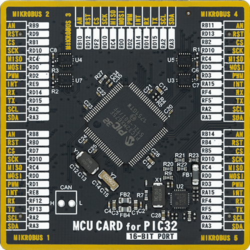
Microcontroller Overview
MCU Card / MCU
Type
8th Generation
Architecture
PIC32
MCU Memory (KB)
512
Silicon Vendor
Microchip
Pin count
100
RAM (Bytes)
65536
Used MCU Pins
mikroBUS™ mapper
Take a closer look
Click board™ Schematic
Step by step
Project assembly

Start by selecting your development board and Click board™. Begin with the UNI-DS v8 as your development board.


Track your results in real time
Application Output
1. Application Output - In Debug mode, the 'Application Output' window enables real-time data monitoring, offering direct insight into execution results. Ensure proper data display by configuring the environment correctly using the provided tutorial.

2. UART Terminal - Use the UART Terminal to monitor data transmission via a USB to UART converter, allowing direct communication between the Click board™ and your development system. Configure the baud rate and other serial settings according to your project's requirements to ensure proper functionality. For step-by-step setup instructions, refer to the provided tutorial.

3. Plot Output - The Plot feature offers a powerful way to visualize real-time sensor data, enabling trend analysis, debugging, and comparison of multiple data points. To set it up correctly, follow the provided tutorial, which includes a step-by-step example of using the Plot feature to display Click board™ readings. To use the Plot feature in your code, use the function: plot(*insert_graph_name*, variable_name);. This is a general format, and it is up to the user to replace 'insert_graph_name' with the actual graph name and 'variable_name' with the parameter to be displayed.

Software Support
Library Description
This library contains API for Hall Switch Click driver.
Key functions:
hallswitch_set_npole- Function for turn on and turn off N Pole
Open Source
Code example
The complete application code and a ready-to-use project are available through the NECTO Studio Package Manager for direct installation in the NECTO Studio. The application code can also be found on the MIKROE GitHub account.
/*!
 * \file
 * \brief Hall Switch Click example
 *
 * # Description
 * The application sets sensor magnetic pole
 *
 * The demo application is composed of two sections :
 *
 * ## Application Init
 * Initializes Driver init and turn OFF S-pole and N-pole
 *
 * ## Application Task
 * Turns S and N on and off every 500 ms
 *
 * \author MikroE Team
 *
 */
// ------------------------------------------------------------------- INCLUDES

#include "board.h"
#include "log.h"
#include "hallswitch.h"

// ------------------------------------------------------------------ VARIABLES

static hallswitch_t hallswitch;
static log_t logger;

// ------------------------------------------------------ APPLICATION FUNCTIONS

void application_init ( void )
{
    log_cfg_t log_cfg;
    hallswitch_cfg_t cfg;

    /**
     * Logger initialization.
     * Default baud rate: 115200
     * Default log level: LOG_LEVEL_DEBUG
     * @note If USB_UART_RX and USB_UART_TX
     * are defined as HAL_PIN_NC, you will
     * need to define them manually for log to work.
     * See @b LOG_MAP_USB_UART macro definition for detailed explanation.
     */
    LOG_MAP_USB_UART( log_cfg );
    log_init( &logger, &log_cfg );
    log_info(&logger, "---- Application Init ----");

    //  Click initialization.

    hallswitch_cfg_setup( &cfg );
    HALLSWITCH_MAP_MIKROBUS( cfg, MIKROBUS_1 );
    hallswitch_init( &hallswitch, &cfg );

    hallswitch_set_npole( &hallswitch, HALLSWITCH_POLE_NO_ACTIVE );
    hallswitch_set_spole( &hallswitch, HALLSWITCH_POLE_NO_ACTIVE );
}

void application_task()
{
    hallswitch_set_npole( &hallswitch, HALLSWITCH_POLE_ACTIVE );
    Delay_ms ( 500 );
    hallswitch_set_spole( &hallswitch, HALLSWITCH_POLE_ACTIVE );
    Delay_ms ( 500 );
    hallswitch_set_npole( &hallswitch, HALLSWITCH_POLE_NO_ACTIVE );
    Delay_ms ( 500 );
    hallswitch_set_spole( &hallswitch, HALLSWITCH_POLE_NO_ACTIVE );
    Delay_ms ( 500 );
}

int main ( void )
{
    /* Do not remove this line or clock might not be set correctly. */
    #ifdef PREINIT_SUPPORTED
    preinit();
    #endif

    application_init( );

    for ( ; ; )
    {
        application_task( );
    }

    return 0;
}


// ------------------------------------------------------------------------ END