Personalize your energy management with LMR36015 and PIC18F86J55
Voltage control at its finest

Published Aug 01, 2023
Click board™
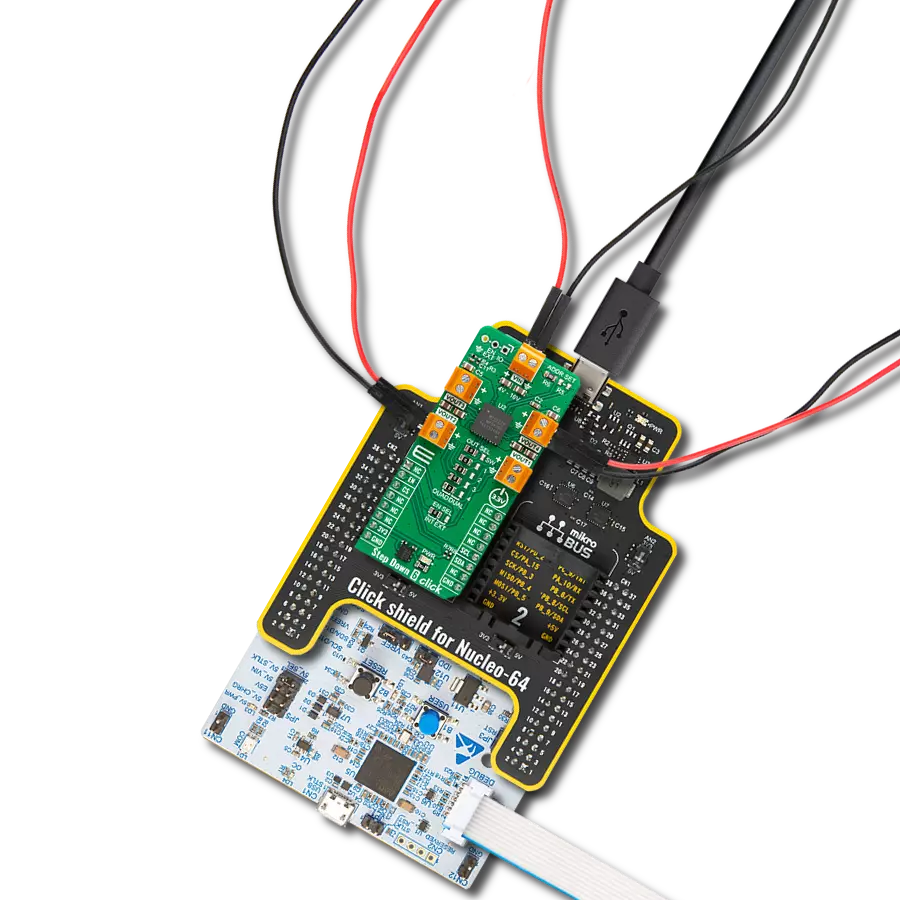
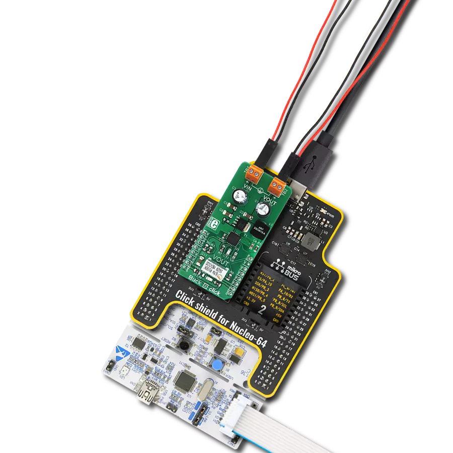
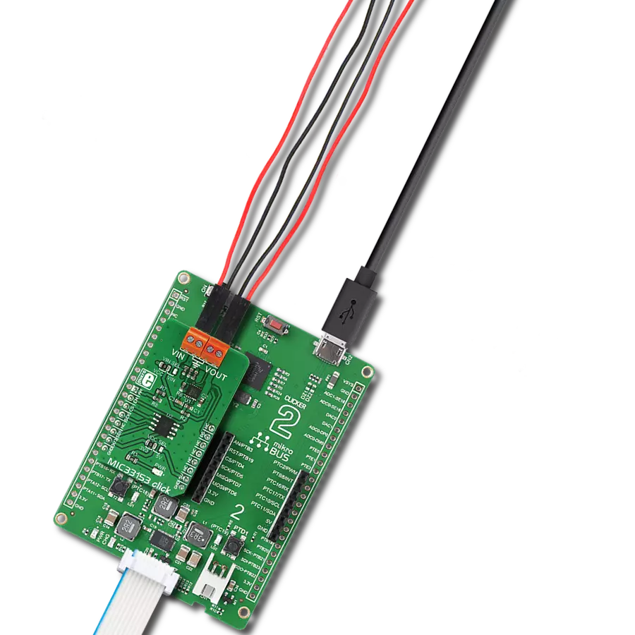
Buck 11 Click
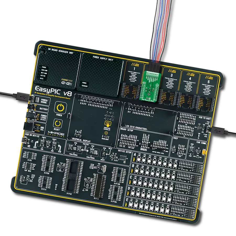
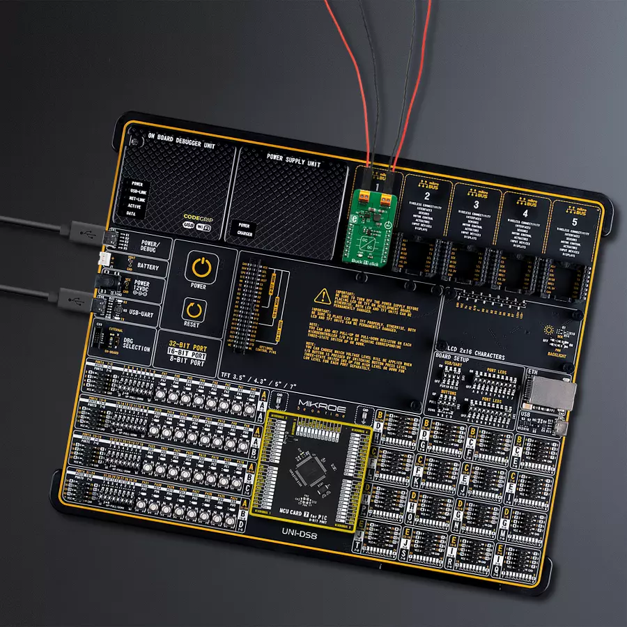
Dev. board
UNI-DS v8
Compiler
NECTO Studio
MCU
PIC18F86J55
Achieve stable and regulated output voltage that matches the specific requirements of electronic devices
A
A
Hardware Overview
How does it work?
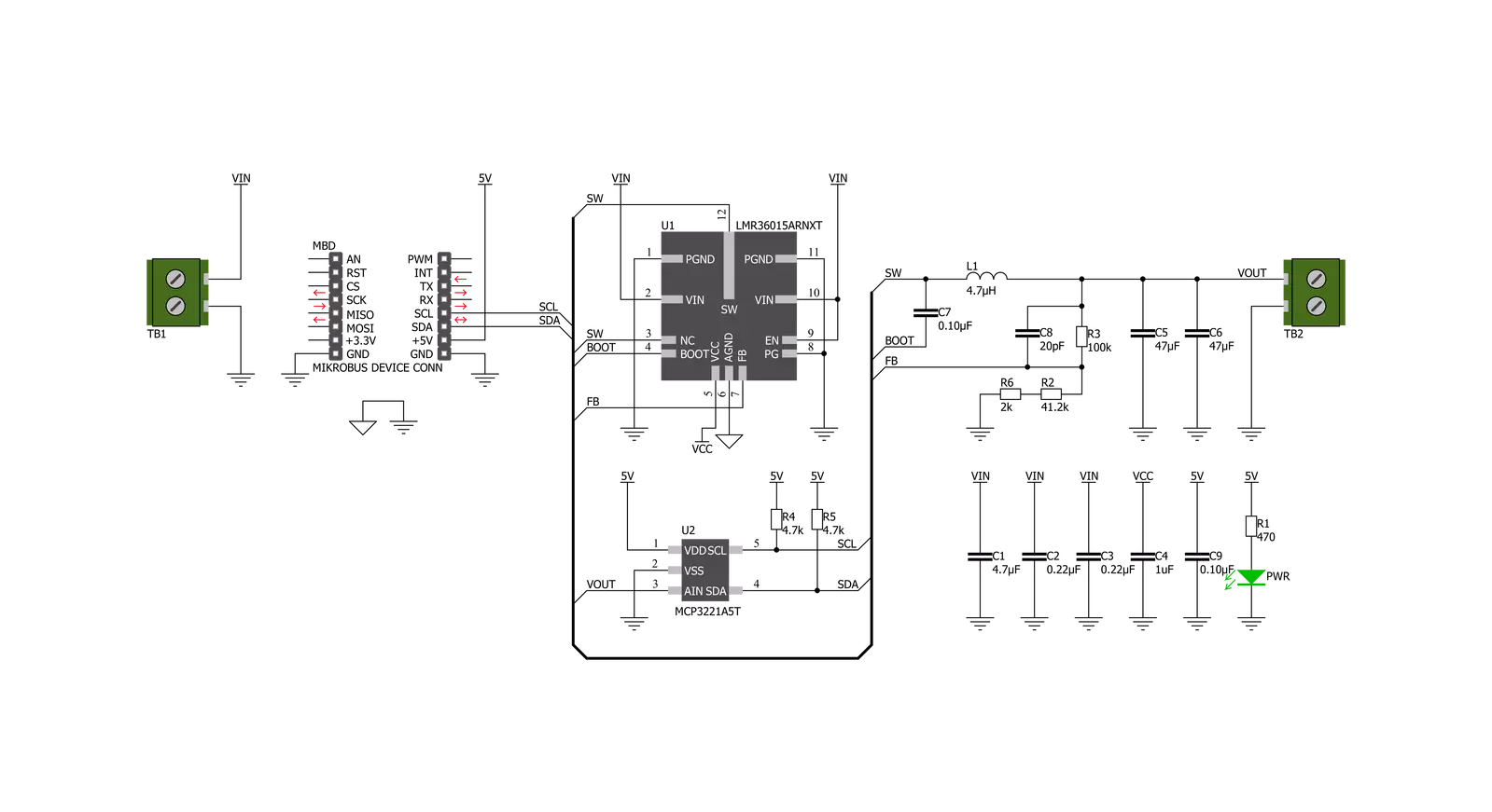
Buck 11 Click is based on the LMR36015, a synchronous step-down converter from Texas Instruments. This advanced integrated step-down converter requires a minimum number of external components readily available on the market. It utilizes a peak-current-mode control architecture, which ensures good efficiency and automatic PFM/PWM mode switching. The LMR36015 buck converter features over-current, under-voltage, and thermal protection, making Buck 11 click a robust and reliable power supply solution. The feedback voltage on the FB pin determines the output voltage. The output voltage is set to 3.3V, making it usable with most embedded applications, allowing them to be powered from the same source, like the rest of the application, which may use a higher voltage for its operation. This is a common-case scenario in various field applications requiring a relatively high voltage, i.e.,
for servos, step motors, displays, and more. When there is an overload at the output, the low-side MOSFET will allow the inductor current to drop. It will remain open until the current through the inductor falls below the limit. If the FB voltage drops too much during the overload, the device enters the hiccup mode, in which the device attempts to periodically restarts itself. The LMR36015 can automatically switch between PWM and PFM modes, depending on the current through the load. At very light loads, the device is operated in PFM mode. In this mode, the high-side MOSFET is operated in bursts, after which the LMR36015 waits for the current through the inductor to drop below the limit. This way, the device is idle while the light load consumes energy stored within the coil. This greatly improves the efficiency when a light load is used. While operated in PWM mode, the output MOSFETs
are driven with the constant PWM frequency of 400kHz, using the pulse width modulation to control the output voltage. This provides good voltage regulation and a low output voltage ripple. Featuring the HotRod™ technology, the LMR36015 occupies a small area on the PCB. Combined with the low count of external components it requires, the LMR36015 leaves enough space for an additional IC to be used. This click uses the MCP3221, a 12-bit A/D converter (ADC) that uses the I2C interface from Microchip. It allows monitoring of the output voltage over the I2C interface. This ADC is powered by the +5V mikroBUS™ power rail. The same voltage is used as a reference. The Click board™ itself requires an external power supply to be connected at the input terminal, labeled as VIN. The VOUT terminal provides the connected load with the regulated 3.3V voltage.

Features overview
Development board
UNI-DS v8 is a development board specially designed for the needs of rapid development of embedded applications. It supports a wide range of microcontrollers, such as different STM32, Kinetis, TIVA, CEC, MSP, PIC, dsPIC, PIC32, and AVR MCUs regardless of their number of pins, and a broad set of unique functions, such as the first-ever embedded debugger/programmer over WiFi. The development board is well organized and designed so that the end-user has all the necessary elements, such as switches, buttons, indicators, connectors, and others, in one place. Thanks to innovative manufacturing technology, UNI-DS v8 provides a fluid and immersive working experience, allowing access anywhere and under any
circumstances at any time. Each part of the UNI-DS v8 development board contains the components necessary for the most efficient operation of the same board. An advanced integrated CODEGRIP programmer/debugger module offers many valuable programming/debugging options, including support for JTAG, SWD, and SWO Trace (Single Wire Output)), and seamless integration with the Mikroe software environment. Besides, it also includes a clean and regulated power supply module for the development board. It can use a wide range of external power sources, including a battery, an external 12V power supply, and a power source via the USB Type-C (USB-C) connector. Communication options such as USB-UART, USB
HOST/DEVICE, CAN (on the MCU card, if supported), and Ethernet is also included. In addition, it also has the well-established mikroBUS™ standard, a standardized socket for the MCU card (SiBRAIN standard), and two display options for the TFT board line of products and character-based LCD. UNI-DS v8 is an integral part of the Mikroe ecosystem for rapid development. Natively supported by Mikroe software tools, it covers many aspects of prototyping and development thanks to a considerable number of different Click boards™ (over a thousand boards), the number of which is growing every day.

Microcontroller Overview
MCU Card / MCU
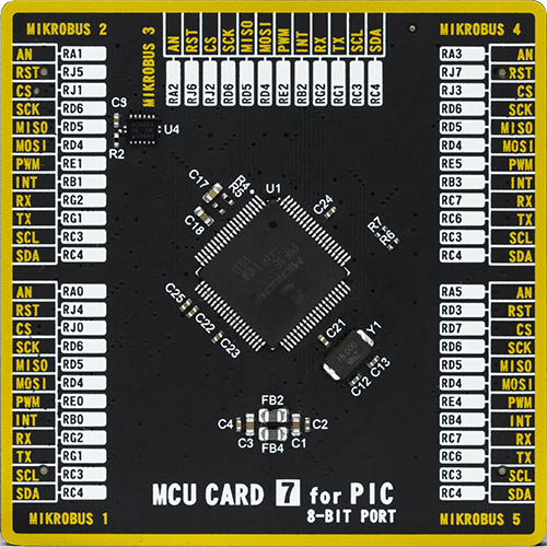
Type
8th Generation
Architecture
PIC
MCU Memory (KB)
96
Silicon Vendor
Microchip
Pin count
80
RAM (Bytes)
3904
Used MCU Pins
mikroBUS™ mapper
Take a closer look
Click board™ Schematic
Step by step
Project assembly

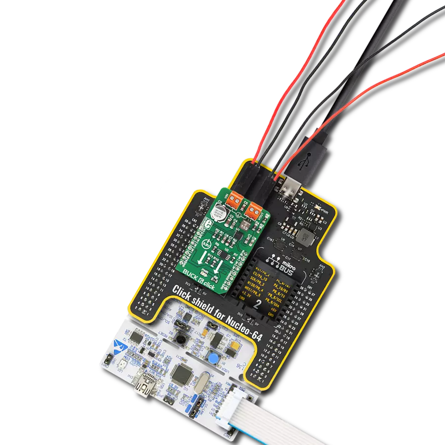
Start by selecting your development board and Click board™. Begin with the UNI-DS v8 as your development board.


Track your results in real time
Application Output
1. Application Output - In Debug mode, the 'Application Output' window enables real-time data monitoring, offering direct insight into execution results. Ensure proper data display by configuring the environment correctly using the provided tutorial.

2. UART Terminal - Use the UART Terminal to monitor data transmission via a USB to UART converter, allowing direct communication between the Click board™ and your development system. Configure the baud rate and other serial settings according to your project's requirements to ensure proper functionality. For step-by-step setup instructions, refer to the provided tutorial.

3. Plot Output - The Plot feature offers a powerful way to visualize real-time sensor data, enabling trend analysis, debugging, and comparison of multiple data points. To set it up correctly, follow the provided tutorial, which includes a step-by-step example of using the Plot feature to display Click board™ readings. To use the Plot feature in your code, use the function: plot(*insert_graph_name*, variable_name);. This is a general format, and it is up to the user to replace 'insert_graph_name' with the actual graph name and 'variable_name' with the parameter to be displayed.

Software Support
Library Description
This library contains API for Buck 11 Click driver.
Key functions:
buck11_read_adc- ADC Read functionbuck11_get_vout- Get VOUT functionbuck11_get_averaged_vout- Get averaged VOUT function
Open Source
Code example
The complete application code and a ready-to-use project are available through the NECTO Studio Package Manager for direct installation in the NECTO Studio. The application code can also be found on the MIKROE GitHub account.
/*!
 * \file
 * \brief Buck11 Click example
 *
 * # Description
 * This aplication control voltage using Buck 11.
 *
 * The demo application is composed of two sections :
 *
 * ## Application Init
 * Initializes I2C serial interface and selects the desired VDD voltage value
 * and VOUT value resolution (to get VOUT value in Volts).
 *
 * ## Application Task
 * Reads the averaged VOUT voltage calculated to Volts by performing a 30 conversions
 * in one measurement cycle. The measured results will be showed on the uart terminal every 300 milliseconds.
 *
 * *note:*
 * The user should measure the VDD voltage value and enter this measured value to the function as VDD value to get
 * more accurate measurement. This VDD voltage is used as reference voltage for the AD conversion.
 *
 * The input voltage (VIN) range is from 4.2V to 60V.
 * The output current (IOUT) value should not be greater than 1.5A.
 *
 * \author MikroE Team
 *
 */
// ------------------------------------------------------------------- INCLUDES

#include "board.h"
#include "log.h"
#include "buck11.h"

// ------------------------------------------------------------------ VARIABLES

static buck11_t buck11;
static log_t logger;

// ------------------------------------------------------ APPLICATION FUNCTIONS

void application_init ( void )
{
    uint8_t vout_resol;
    log_cfg_t log_cfg;
    buck11_cfg_t cfg;

    /**
     * Logger initialization.
     * Default baud rate: 115200
     * Default log level: LOG_LEVEL_DEBUG
     * @note If USB_UART_RX and USB_UART_TX
     * are defined as HAL_PIN_NC, you will
     * need to define them manually for log to work.
     * See @b LOG_MAP_USB_UART macro definition for detailed explanation.
     */
    LOG_MAP_USB_UART( log_cfg );
    log_init( &logger, &log_cfg );
    log_info( &logger, "---- Application Init ----" );

    //  Click initialization.

    buck11_cfg_setup( &cfg );
    BUCK11_MAP_MIKROBUS( cfg, MIKROBUS_1 );
    buck11_init( &buck11, &cfg );

    Delay_ms ( 500 );

    buck11_set_vdd_value( 4.935 );
    vout_resol = BUCK11_VOUT_VOLTS;

    log_printf( &logger, "** Buck 11 is initialized ** \r\n" );
    log_printf( &logger, "************************************* \r\n" );
    Delay_ms ( 200 );
}

void application_task ( )
{
    float vout_value;
    uint8_t vout_resol;

    vout_value = buck11_get_averaged_vout( &buck11, vout_resol, 30 );

    log_printf( &logger, "VOUT: %f", vout_value );

    if ( vout_resol == BUCK11_VOUT_VOLTS )
    {
        log_printf( &logger, " V \r\n" );
    }
    else
    {
        log_printf( &logger, " mV \r\n" );
    }

    log_printf( &logger, "************************************* \r\n" );
    Delay_ms ( 300 );
}

int main ( void )
{
    /* Do not remove this line or clock might not be set correctly. */
    #ifdef PREINIT_SUPPORTED
    preinit();
    #endif

    application_init( );

    for ( ; ; )
    {
        application_task( );
    }

    return 0;
}


// ------------------------------------------------------------------------ END