Unlock the full potential of PWM with LTC8500 and PIC32MZ1024EFK144
48 channels, 1 SPI connection - Unleash your creativity!

Published Oct 17, 2023
Click board™
PWM 2 Click
Dev Board
UNI-DS v8
Compiler
NECTO Studio
MCU
PIC32MZ1024EFK144
With 48 channels controlled through one interface, you gain total PWM dominance, giving you the power to manage your devices and applications with precision and efficiency
A
A
Hardware Overview
How does it work?
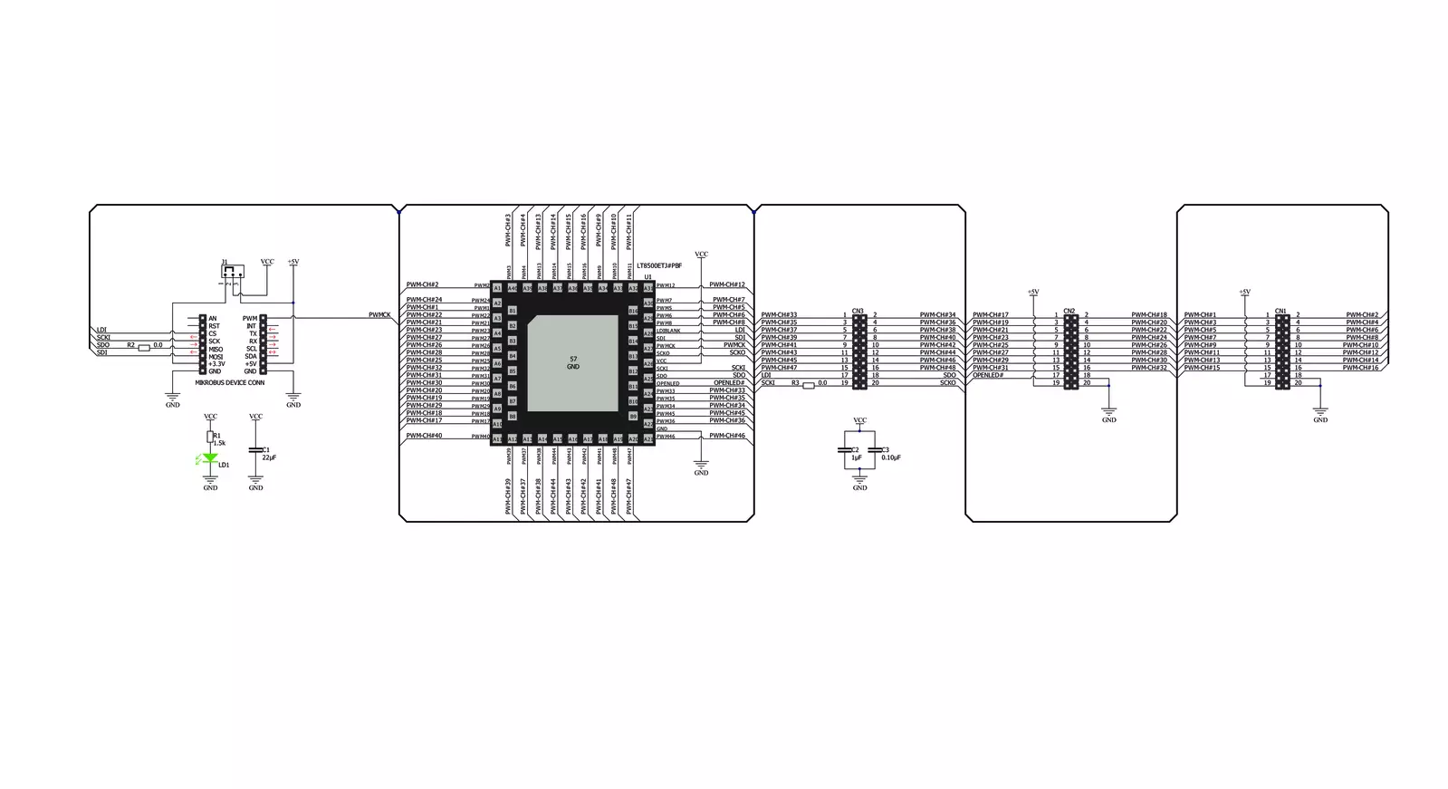
PWM 2 Click is based on the LT8500, a 48-channel LED PWM generator with 12-bit resolution and 50MHz serial interface from Analog Devices. This IC has 48 independent 12-bit PWM channels, each with 6-bit correction up to 50% of the original duty cycle. The LT8500 IC is clocked by a clock signal at the PWMCK pin. The frequency of the clock signal can go up to 25MHz, generating the PWM output frequency of up to 6.1kHz, which is sufficient for most purposes. The maximum speed of the LT8500 serial interface goes up to 50MHz in theory, but in practice, it will depend on many factors. The clock signal at the PWM pin of the mikroBUS™ is triggering an internal counter register (PWMCK). This register is compared with the content of the PWMRSYNC register, associated with each channel. Whenever the counter value is less than the value written in a specific channel PWMRSYNC register, the PWM output of that channel goes to a HIGH logic level. The frequency of the output PWM signal is therefore determined by the frequency the clock signal at the PWMCK pin. This represents the basic operating principle of the LTC8500 IC. The PWMCK pin is routed to the PWM pin of the mikroBUS™. The device uses an industry-standard SPI interface for the communication. The LDI pin acts as the normal Chip Select, latching the SPI data in, but it has an additional function if held to a HIGH logic level
for more than 50µs. In that case, the IC will be reset, and all outputs will be blanked. Therefore, care should be taken not to hold this pin to a HIGH logic level, for more than 5µs. The LDI pin is routed to the CS pin of the mikroBUS™ and it is labeled as LDI. Besides the usual SPI interface lines, the LT8500 PWM generator IC provides a serial interface clock output signal (SCKO), allowing additional devices to be connected in the parallel 5-wire topology (LDI, SCKI, SDI, SDO, and SCKO). This allows large-scale cascading, without the need for the skew balancing or buffering the signals. These additional pins are available at the standard 2.54 pitch headers on board. These additional pins on the header are described in a table, below. More information about cascading and using the SCKO feature of the IC can be found in the LT8500 datasheet. The device is controlled by sending commands via the SPI interface, embedded in a command frame. There are eight different commands which are used to control the following parameters: PWM outputs update (synchronously or asynchronously to PWM period), the dot correction factor, self-test initialization, phase shifting between banks (groups of 16 channels), enabling/ disabling of the PWM output drivers, and enabling/disabling of the dot correction . A frame consists of a 12-bit data field for each of the 48 PWM channels, followed by an
8-bit command field, which contains one of the eight command codes. The status frame is clocked on the SDO pin, providing the host MCU with the frame information: LED fault status, phase shifting status, correction status, synchronization status, and so on. This information can be used either for troubleshooting or for other purposes by the host MCU application. As already mentioned, additional functionalities of the LT8500 IC are offered via the onboard headers, along with the 48 PWM channel outputs. The outputs are not meant to drive devices with high current, so PWM 2 click is best used as the driver for additional circuitry, whether it is a simple MOSFET LED driver, or a more complex ICs, such as the LT3595A LED driver, for which a special input pin is reserved, allowing open LED conditions to be detected, even on the externally connected LT3595 IC. Onboard headers also offer fixed 5V output from the mikroBUS™ for the auxiliary purposes. This Click board™ can operate with either 3.3V or 5V logic voltage levels selected via the PWR SEL jumper. This way, both 3.3V and 5V capable MCUs can use the communication lines properly. Also, this Click board™ comes equipped with a library containing easy-to-use functions and an example code that can be used as a reference for further development.


Features overview
Development board
UNI-DS v8 is a development board specially designed for the needs of rapid development of embedded applications. It supports a wide range of microcontrollers, such as different STM32, Kinetis, TIVA, CEC, MSP, PIC, dsPIC, PIC32, and AVR MCUs regardless of their number of pins, and a broad set of unique functions, such as the first-ever embedded debugger/programmer over WiFi. The development board is well organized and designed so that the end-user has all the necessary elements, such as switches, buttons, indicators, connectors, and others, in one place. Thanks to innovative manufacturing technology, UNI-DS v8 provides a fluid and immersive working experience, allowing access anywhere and under any
circumstances at any time. Each part of the UNI-DS v8 development board contains the components necessary for the most efficient operation of the same board. An advanced integrated CODEGRIP programmer/debugger module offers many valuable programming/debugging options, including support for JTAG, SWD, and SWO Trace (Single Wire Output)), and seamless integration with the Mikroe software environment. Besides, it also includes a clean and regulated power supply module for the development board. It can use a wide range of external power sources, including a battery, an external 12V power supply, and a power source via the USB Type-C (USB-C) connector. Communication options such as USB-UART, USB
HOST/DEVICE, CAN (on the MCU card, if supported), and Ethernet is also included. In addition, it also has the well-established mikroBUS™ standard, a standardized socket for the MCU card (SiBRAIN standard), and two display options for the TFT board line of products and character-based LCD. UNI-DS v8 is an integral part of the Mikroe ecosystem for rapid development. Natively supported by Mikroe software tools, it covers many aspects of prototyping and development thanks to a considerable number of different Click boards™ (over a thousand boards), the number of which is growing every day.

Microcontroller Overview
MCU Card / MCU
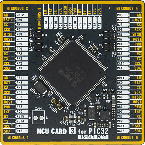
Type
8th Generation
Architecture
PIC32
MCU Memory (KB)
1024
Silicon Vendor
Microchip
Pin count
144
RAM (Bytes)
262144
Used MCU Pins
mikroBUS™ mapper
Take a closer look
Schematic
Step by step
Project assembly

Start by selecting your development board and Click board™. Begin with the UNI-DS v8 as your development board.


Track your results in real time
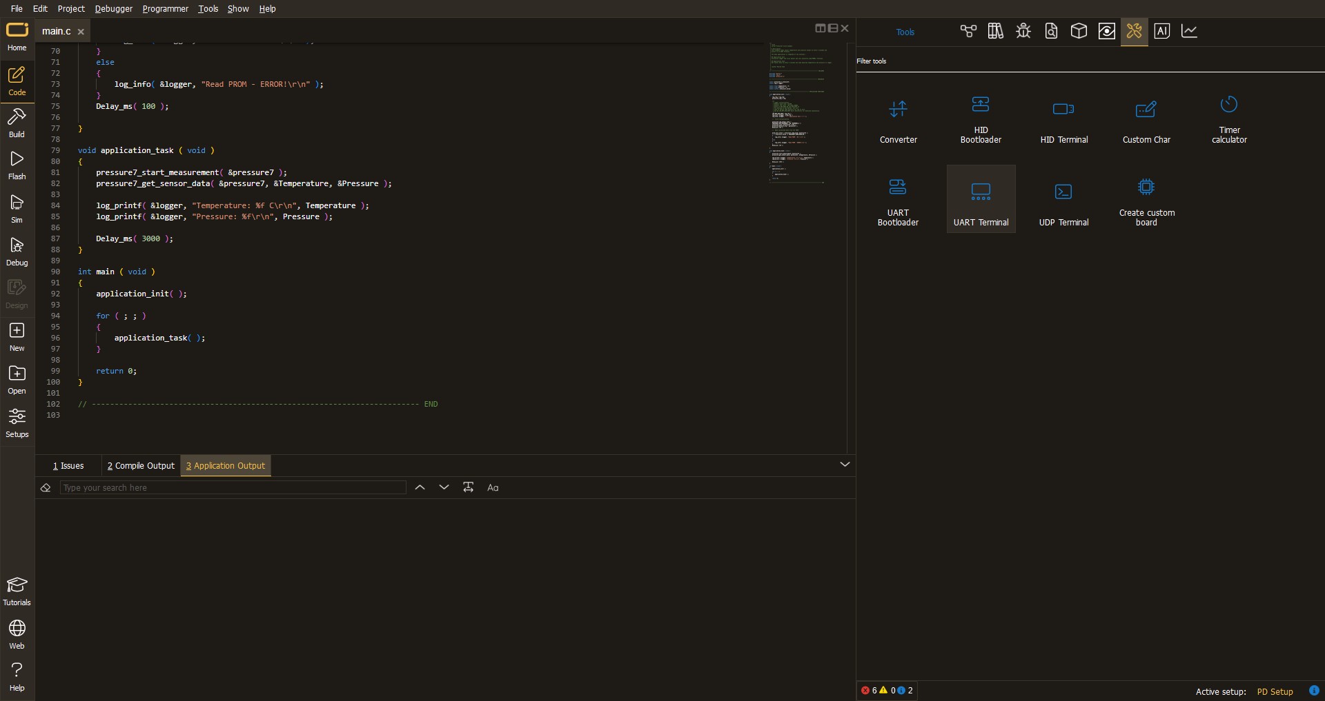
Application Output
After pressing the "FLASH" button on the left-side panel, it is necessary to open the UART terminal to display the achieved results. By clicking on the Tools icon in the right-hand panel, multiple different functions are displayed, among which is the UART Terminal. Click on the offered "UART Terminal" icon.
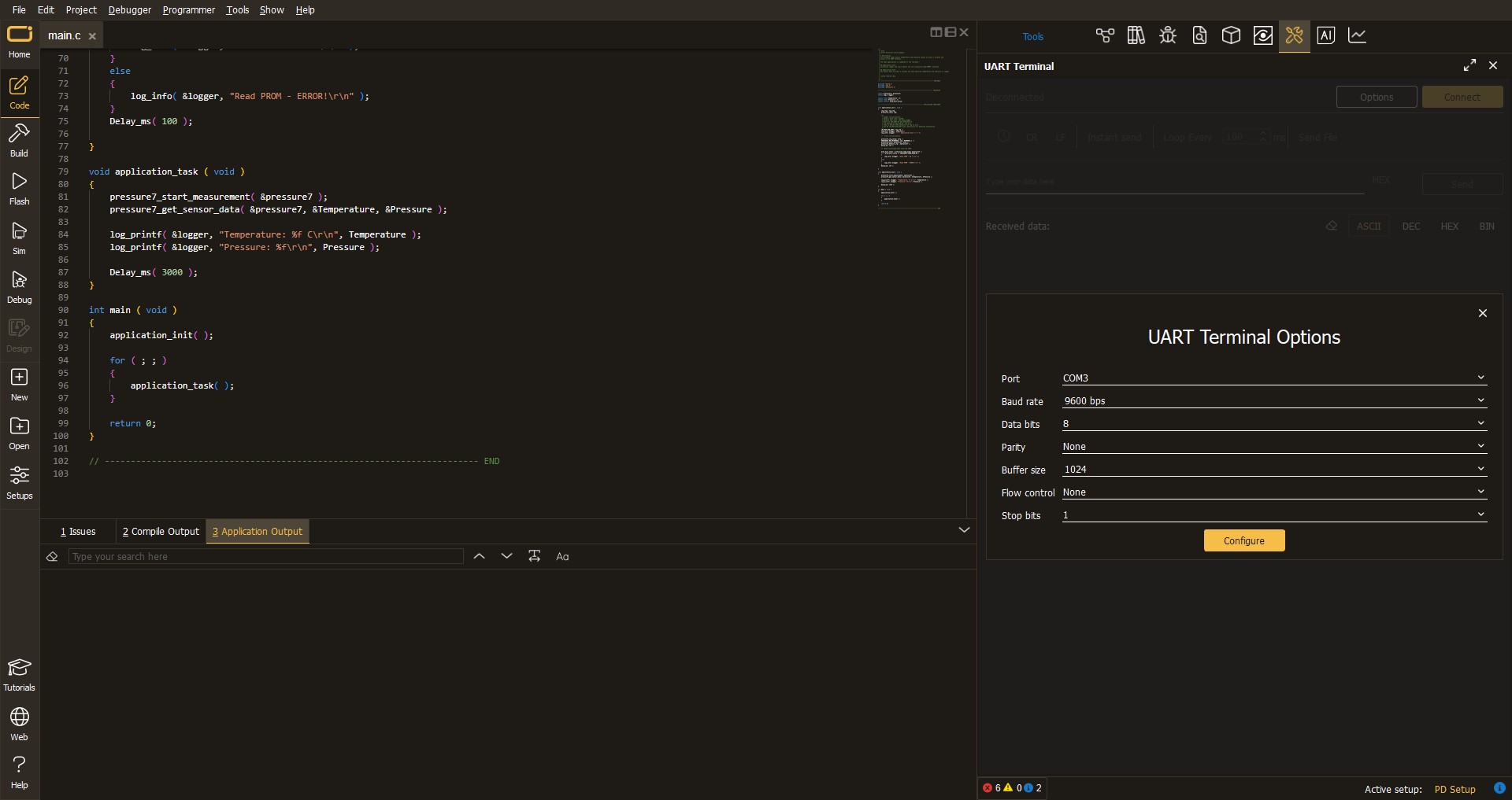
Once the UART terminal is opened, the window takes on a new form. At the top of the tab are two buttons, one for adjusting the parameters of the UART terminal and the other for connecting the UART terminal. The tab's lower part is reserved for displaying the achieved results. Before connecting, the terminal has a Disconnected status, indicating that the terminal is not yet active. Before connecting, it is necessary to check the set parameters of the UART terminal. Click on the "OPTIONS" button.
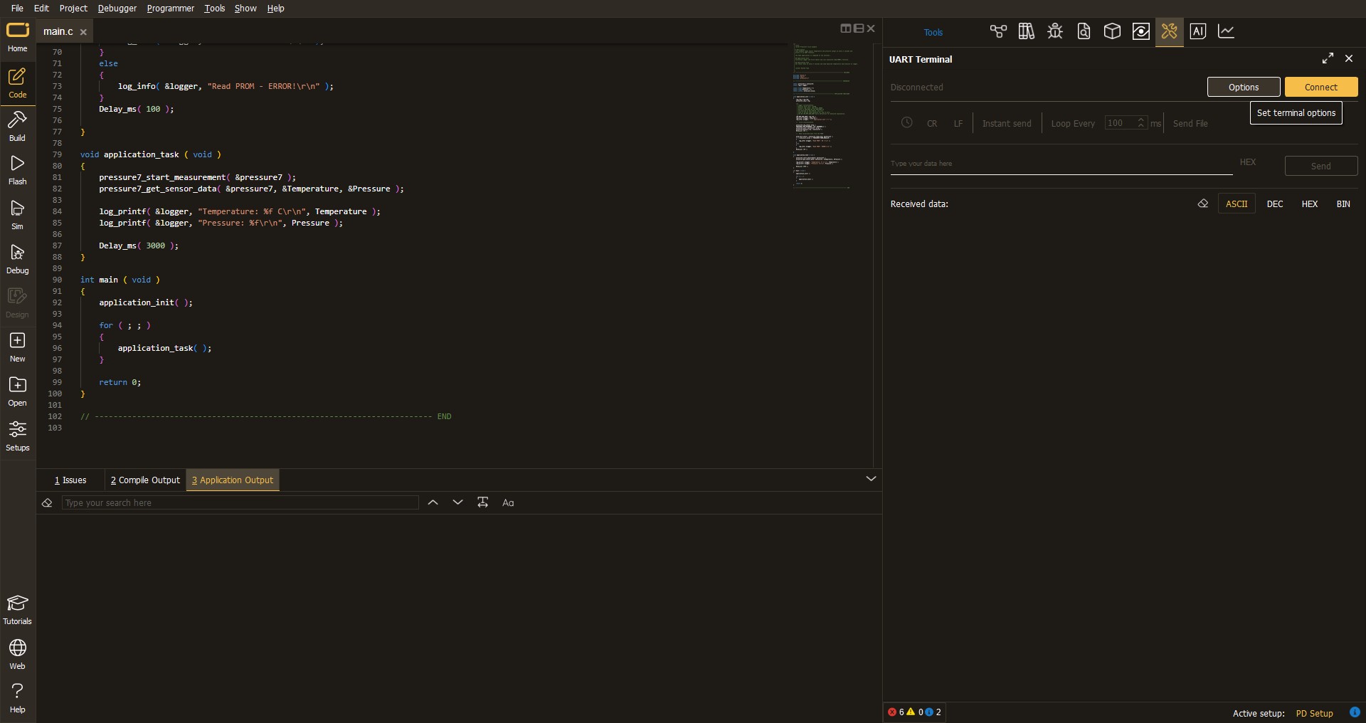
In the newly opened UART Terminal Options field, we check if the terminal settings are correct, such as the set port and the Baud rate of UART communication. If the data is not displayed properly, it is possible that the Baud rate value is not set correctly and needs to be adjusted to 115200. If all the parameters are set correctly, click on "CONFIGURE".
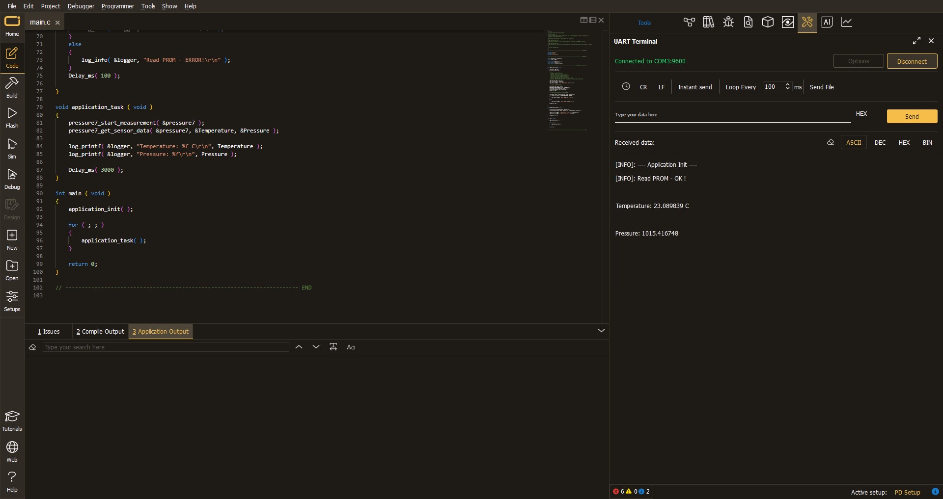
The next step is to click on the "CONNECT" button, after which the terminal status changes from Disconnected to Connected in green, and the data is displayed in the Received data field.
Software Support
Library Description
This library contains API for PWM 2 Click driver.
Key functions:
pwm2_set_channel- Set channel function.pwm2_pwm_start- Start PWM module.send_output_enable_frame- Enable frame.
Open Source
Code example
This example can be found in NECTO Studio. Feel free to download the code, or you can copy the code below.
/*!
 * \file
 * \brief Pwm2 Click example
 *
 * # Description
 * This application send the PWM signal in one or more outputs.
 *
 * The demo application is composed of two sections :
 *
 * ## Application Init
 * Configures the click board and sets all PWM channels on the click board to
 * 50% duty cycle with the phase shift enabled.
 *
 * ## Application Task
 * The first 10 PWM channels of PWM2 Click board are switched back and forth
 * from 25% duty cycle to 75% duty cycle every 10 seconds.
 *
 * \author MikroE Team
 *
 */
// ------------------------------------------------------------------- INCLUDES

#include "board.h"
#include "pwm2.h"

// ------------------------------------------------------------------ VARIABLES

static pwm2_t pwm2;

void application_init ( void )
{
    pwm2_cfg_t cfg;

    //  Click initialization.

    pwm2_cfg_setup( &cfg );
    PWM2_MAP_MIKROBUS( cfg, MIKROBUS_1 );
    pwm2_init( &pwm2, &cfg );

    pwm2_set_duty_cycle( &pwm2, 0.5 );
    pwm2_pwm_start( &pwm2 );

    pwm2_default_cfg( &pwm2 );
    pwm2_toggle_phase_shift( &pwm2 );

    //setting all 48 PWM channels of the PWM2 click to 50% duty
    for( uint8_t cnt = 1; cnt < 49; cnt++ )
    {
        pwm2_set_channel( &pwm2, cnt, PWM2_50_PERCENT_DUTY, PWM2_NO_CORRECTION );
    }
}

void application_task ( void )
{
    for ( uint8_t cnt = 1; cnt < 10; cnt++ )
    {
        pwm2_set_channel( &pwm2, cnt, PWM2_25_PERCENT_DUTY, PWM2_NO_CORRECTION );
    }
    Delay_ms( 10000 );

    for ( uint8_t cnt = 1; cnt < 10; cnt++ )
    {
        pwm2_set_channel( &pwm2, cnt, PWM2_75_PERCENT_DUTY, PWM2_NO_CORRECTION );
    }
    Delay_ms( 10000 );
}

void main ( void )
{
    application_init( );

    for ( ; ; )
    {
        application_task( );
    }
}


// ------------------------------------------------------------------------ END


