Create contactless switches for applications where physical contact is impractical or undesirable with NMH1000 and PIC18F86K22
Hall-effect magnetic switch

Published Jan 23, 2024
Click board™
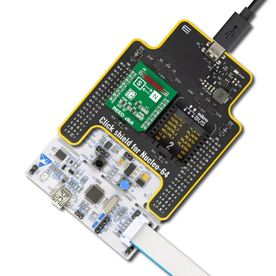
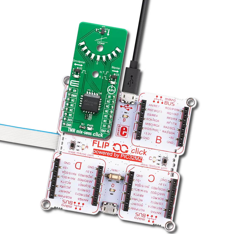
Hall Switch 3 Click
Dev. board
UNI-DS v8
Compiler
NECTO Studio
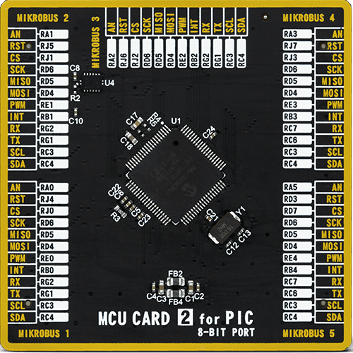
MCU
PIC18F86K22
Detect changes in vertical magnetic fields and achieve unparalleled sensitivity to specific magnet orientations
A
A
Hardware Overview
How does it work?
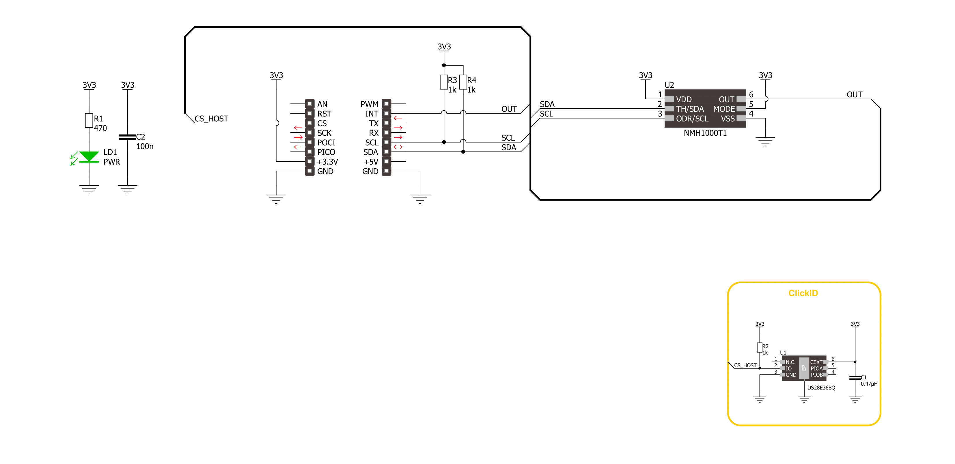
Hall Switch 3 Click is based on the NMH1000, a Hall-effect magnetic switch from NXP Semiconductor. The switch processes its input over the functional blocks that consist of a configurable state machine, an analog-to-voltage conversion of the input, and a comparison to generate the bi-state output. The output is arranged in a linear succession. The NMH1000 has a transducer that generates a small charge proportional to the
proximal magnetic flux density. The Hall-effect charge is converted to voltage and compared with the pre-defined threshold voltage. This determines the state of the switch's output. Hall Switch 3 Click uses a standard 2-wire I2C interface to communicate with the host MCU, supporting a clock frequency of up to 1MHz. The output of the switch, according to the pre-defined threshold, is available over the output OUT pin. This Click
board™ can be operated only with a 3.3V logic voltage level. The board must perform appropriate logic voltage level conversion before using MCUs with different logic levels. Also, it comes equipped with a library containing functions and an example code that can be used as a reference for further development.

Features overview
Development board
UNI-DS v8 is a development board specially designed for the needs of rapid development of embedded applications. It supports a wide range of microcontrollers, such as different STM32, Kinetis, TIVA, CEC, MSP, PIC, dsPIC, PIC32, and AVR MCUs regardless of their number of pins, and a broad set of unique functions, such as the first-ever embedded debugger/programmer over WiFi. The development board is well organized and designed so that the end-user has all the necessary elements, such as switches, buttons, indicators, connectors, and others, in one place. Thanks to innovative manufacturing technology, UNI-DS v8 provides a fluid and immersive working experience, allowing access anywhere and under any
circumstances at any time. Each part of the UNI-DS v8 development board contains the components necessary for the most efficient operation of the same board. An advanced integrated CODEGRIP programmer/debugger module offers many valuable programming/debugging options, including support for JTAG, SWD, and SWO Trace (Single Wire Output)), and seamless integration with the Mikroe software environment. Besides, it also includes a clean and regulated power supply module for the development board. It can use a wide range of external power sources, including a battery, an external 12V power supply, and a power source via the USB Type-C (USB-C) connector. Communication options such as USB-UART, USB
HOST/DEVICE, CAN (on the MCU card, if supported), and Ethernet is also included. In addition, it also has the well-established mikroBUS™ standard, a standardized socket for the MCU card (SiBRAIN standard), and two display options for the TFT board line of products and character-based LCD. UNI-DS v8 is an integral part of the Mikroe ecosystem for rapid development. Natively supported by Mikroe software tools, it covers many aspects of prototyping and development thanks to a considerable number of different Click boards™ (over a thousand boards), the number of which is growing every day.

Microcontroller Overview
MCU Card / MCU
Type
8th Generation
Architecture
PIC
MCU Memory (KB)
64
Silicon Vendor
Microchip
Pin count
80
RAM (Bytes)
3862
Used MCU Pins
mikroBUS™ mapper
Take a closer look
Click board™ Schematic
Step by step
Project assembly

Start by selecting your development board and Click board™. Begin with the UNI-DS v8 as your development board.


Track your results in real time
Application Output
1. Application Output - In Debug mode, the 'Application Output' window enables real-time data monitoring, offering direct insight into execution results. Ensure proper data display by configuring the environment correctly using the provided tutorial.

2. UART Terminal - Use the UART Terminal to monitor data transmission via a USB to UART converter, allowing direct communication between the Click board™ and your development system. Configure the baud rate and other serial settings according to your project's requirements to ensure proper functionality. For step-by-step setup instructions, refer to the provided tutorial.

3. Plot Output - The Plot feature offers a powerful way to visualize real-time sensor data, enabling trend analysis, debugging, and comparison of multiple data points. To set it up correctly, follow the provided tutorial, which includes a step-by-step example of using the Plot feature to display Click board™ readings. To use the Plot feature in your code, use the function: plot(*insert_graph_name*, variable_name);. This is a general format, and it is up to the user to replace 'insert_graph_name' with the actual graph name and 'variable_name' with the parameter to be displayed.

Software Support
Library Description
This library contains API for Hall Switch 3 Click Click driver.
Key functions:
hallswitch3_get_mag_data- This function is used to indicates a relative magnetic field strength.hallswitch3_set_out_data_rate- This function provides the capability for the user to override the fixed sample rate controlling the sleep-compare-Vout cycle time.hallswitch3_get_status- This function reads a status reporting of modes and selections.
Open Source
Code example
The complete application code and a ready-to-use project are available through the NECTO Studio Package Manager for direct installation in the NECTO Studio. The application code can also be found on the MIKROE GitHub account.
/*!
 * @file main.c
 * @brief Hall Switch 3 Click example
 *
 * # Description
 * This example demonstrates the use of Hall Switch 3 Click board
 * by reading and displaying the magnetic field strength value.
 *
 * The demo application is composed of two sections :
 *
 * ## Application Init
 * Initialization of I2C module and log UART.
 * After driver initialization, the app executes a default configuration.
 *
 * ## Application Task
 * This example demonstrates the use of the Hall Switch 3 Click board.
 * The demo application reads and displays the relative magnetic field strength value [Gaussian units]
 * and detects when the magnetic field strength is not in the configured range.
 * The results are sent to the UART terminal, where you can monitor their changes.
 *
 * @author Nenad Filipovic
 *
 */

#include "board.h"
#include "log.h"
#include "hallswitch3.h"

static hallswitch3_t hallswitch3;
static log_t logger;

void application_init ( void )
{
    log_cfg_t log_cfg;  /**< Logger config object. */
    hallswitch3_cfg_t hallswitch3_cfg;  /**< Click config object. */

    /**
     * Logger initialization.
     * Default baud rate: 115200
     * Default log level: LOG_LEVEL_DEBUG
     * @note If USB_UART_RX and USB_UART_TX
     * are defined as HAL_PIN_NC, you will
     * need to define them manually for log to work.
     * See @b LOG_MAP_USB_UART macro definition for detailed explanation.
     */
    LOG_MAP_USB_UART( log_cfg );
    log_init( &logger, &log_cfg );
    log_info( &logger, " Application Init " );

    // Click initialization.
    hallswitch3_cfg_setup( &hallswitch3_cfg );
    HALLSWITCH3_MAP_MIKROBUS( hallswitch3_cfg, MIKROBUS_1 );
    if ( I2C_MASTER_ERROR == hallswitch3_init( &hallswitch3, &hallswitch3_cfg ) )
    {
        log_error( &logger, " Communication init." );
        for ( ; ; );
    }

    if ( HALLSWITCH3_ERROR == hallswitch3_default_cfg ( &hallswitch3 ) )
    {
        log_error( &logger, " Default configuration." );
        for ( ; ; );
    }

    log_info( &logger, " Application Task " );
}

void application_task ( void )
{
    int8_t mag_data = 0;
    if ( HALLSWITCH3_OK == hallswitch3_get_mag_data( &hallswitch3, &mag_data ) )
    {
        log_printf( &logger, " Magnetic Field: %d [Gs]\r\n", ( int16_t ) mag_data );
        if ( HALLSWITCH3_OUT_STATE_LOW == hallswitch3_check_mag_field( &hallswitch3 ) )
        {
            log_printf( &logger, " The switch is open.\r\n" );
        }
    }
    Delay_ms ( 1000 );
}

int main ( void )
{
    /* Do not remove this line or clock might not be set correctly. */
    #ifdef PREINIT_SUPPORTED
    preinit();
    #endif

    application_init( );

    for ( ; ; )
    {
        application_task( );
    }

    return 0;
}

// ------------------------------------------------------------------------ END