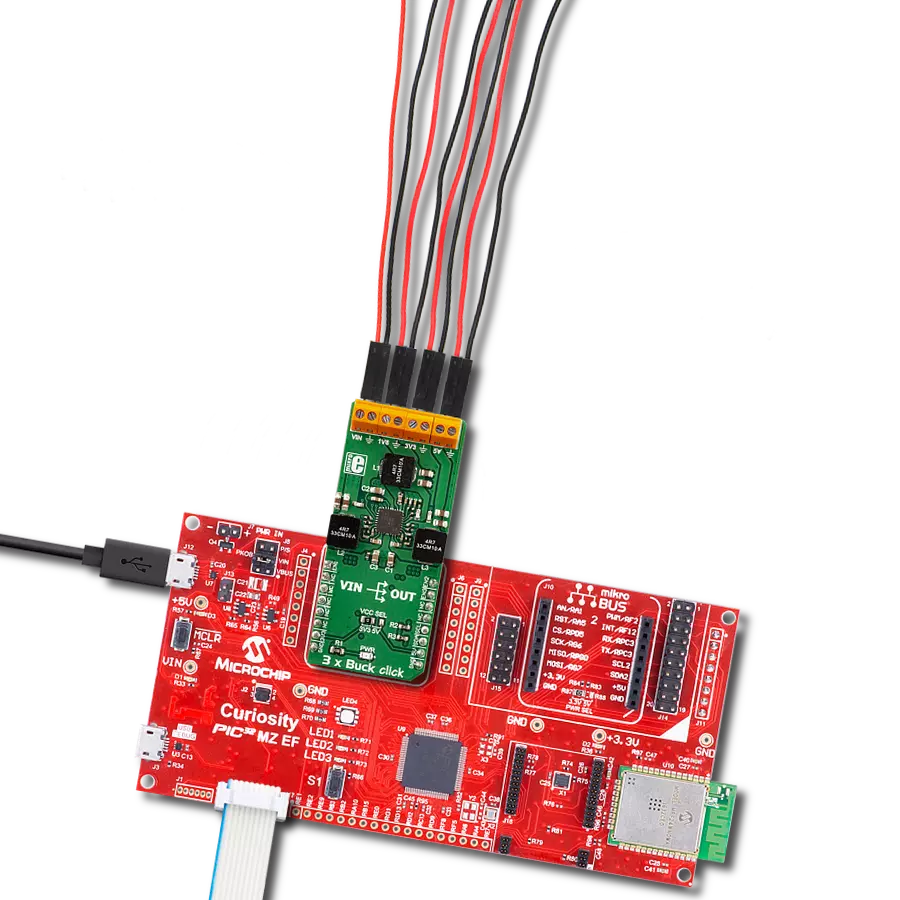
Upgrade your power needs with triple step-down conversion based on TPS65263 and PIC32MZ1024EFH064
Buck it right, save power

Published Jul 31, 2023
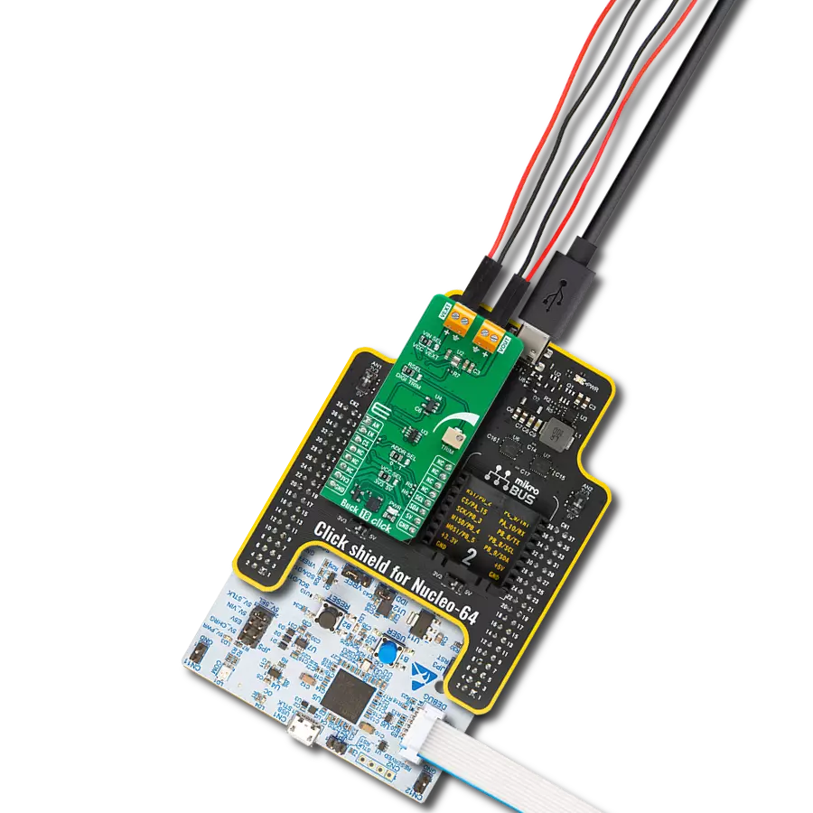
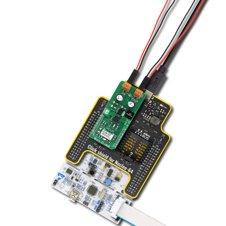
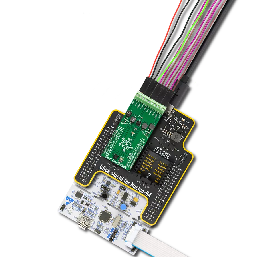
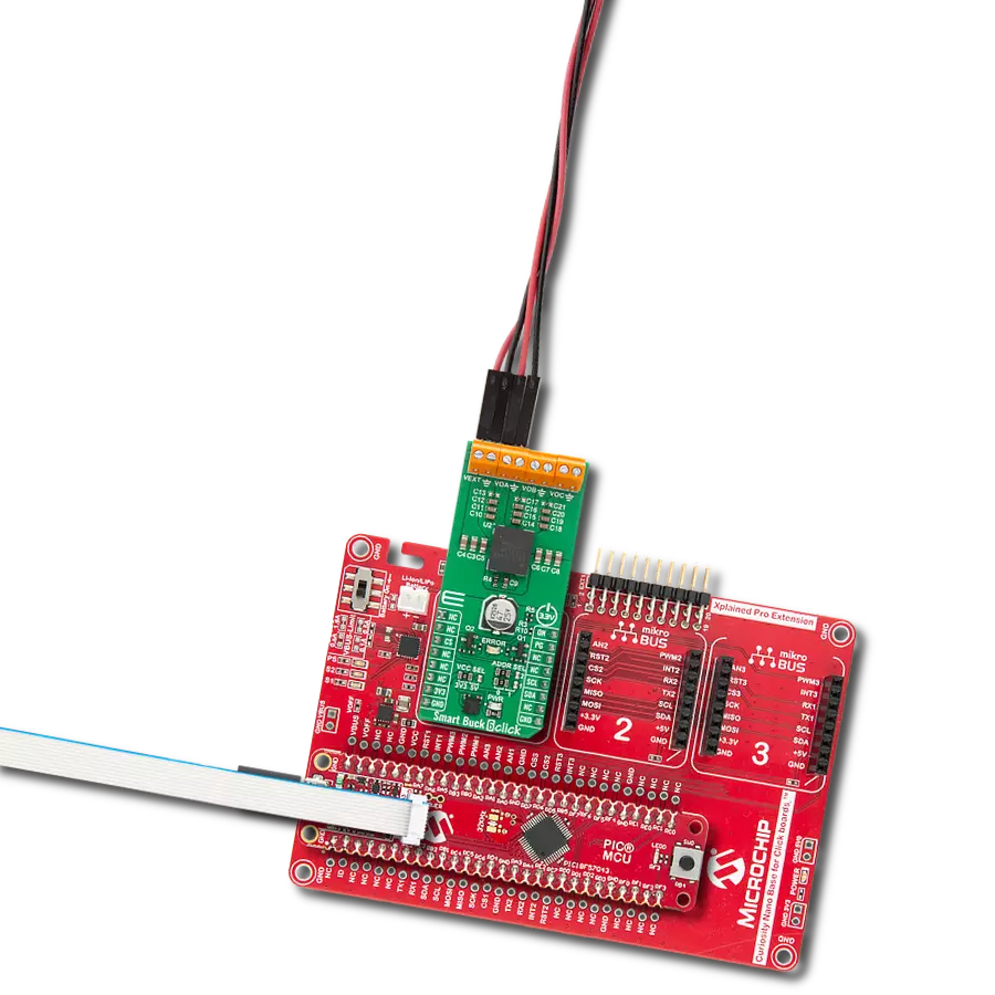
Click board™
3xBuck click
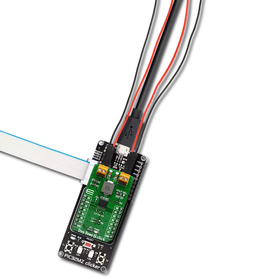
Dev. board
PIC32MZ clicker
Compiler
NECTO Studio
MCU
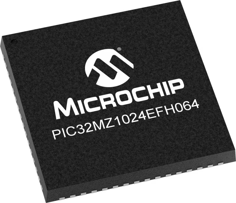
PIC32MZ1024EFH064
Offering voltage control at your fingertips, this cutting-edge solution empowers your gadgets to perform at their best
A
A
Hardware Overview
How does it work?
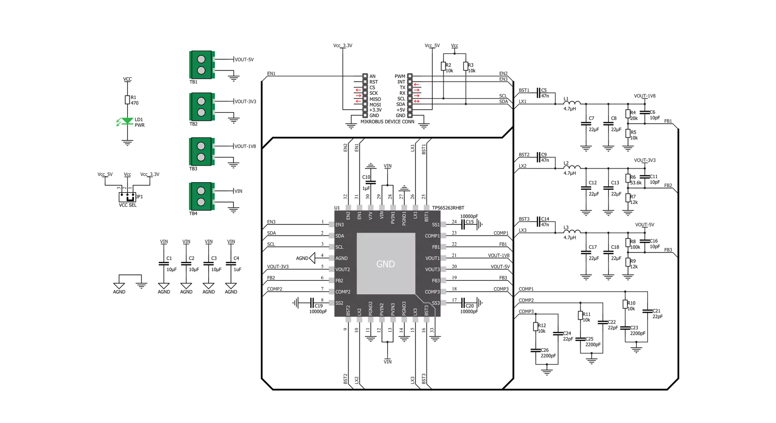
3xBuck Click is based on the TPS65263, a triple synchronous step-down converter from Texas Instruments with programmable dynamic voltage scaling. This IC contains three independent switching sections, which operate at a fixed frequency of 600kHz. One buck section uses the switching clock, which is 180˚ out-of-phase, with respect to the other two sections. This ensures low input current ripple, as well as the lowered EMI of the power supply itself. The TPS65263 IC has the I2C bus logic section, which allows the output voltage of each converter to be programmed. The output voltage is initially set with feedback voltage divider resistors on each section. The output voltages of the sections are set to 5V, 3.3V, and 1.8V because these values are the most commonly used in embedded applications. As soon as the command is sent via the I2C interface, the logic section of the TPS65263 IC takes over the control, allowing to program the voltage at each of the three outputs between 0.68V to 1.95V, with 10mV steps. This allows the desired output to be fine-tuned according to the application's specific needs, which is powered by the 3xBuck click. The I2C interface is also used to independently retrieve
the Power Good status, the overcurrent, and the die temperature warning for each buck section. There are three completely independent switching sections in the TPS65263 IC, meaning each has its dedicated Enable pin, Soft-Start pin, and loop compensation pin. The Enable pins for each section are routed to mikroBUS™. EN1, EN2, and EN3 are routed to AN, PWM, and INT pins of the mikroBUS™, respectively. This allows the host MCU to control the operation of the 3xBuck Click. Not all three sections share the same characteristics. The output of the 3xBuck click labeled as 1V8 (VOUT1) can withstand up to 3A of current while supplied with 12V across the input terminal. The other two outputs can deliver up to 2A, keeping the output well regulated, well within the 1% margin. However, it should be noted that this is the combined current rating, so if multiple outputs are used, the summed current consumption should not exceed these values. The input voltage should range between 4.5V and 18V, with a remark that it must be sufficiently higher than the selected output voltage to reach the specified voltage and current ratings. The soft-start feature uses a 10nF capacitor at the
dedicated SS pin. Each channel has its own dedicated SS pin, so three pins are used to set the soft start of each channel. The soft-start function prevents the high inrush current on power up, ramping up the output current during the soft-start period, defined by the capacitor. As mentioned, the device features protection functions that allow reliable operation in events such as short circuit protection, overcurrent, overvoltage, and thermal protection. If the connected load draws too much current, the cycle-by-cycle current limit will be activated on both high- and low-side output MOSFETs. If the high current condition persists after 0.5ms, the device will enter the hiccup mode, shutting down completely, then restarting after 14ms. The whole startup sequence will be repeated; if the fault condition persists on the output, this cycle will be repeated. This prevents damage in the case of significant loads connected at the output. The logic voltage level of the 3xBuck click can be selected by switching the SMD jumper labeled VCC SEL to an appropriate position. This allows interfacing with both 3.3V and 5V MCUs, expanding the interfacing options of this board.

Features overview
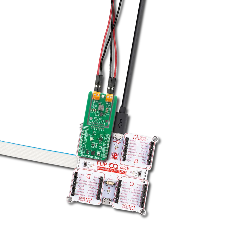
Development board
PIC32MZ Clicker is a compact starter development board that brings the flexibility of add-on Click boards™ to your favorite microcontroller, making it a perfect starter kit for implementing your ideas. It comes with an onboard 32-bit PIC32MZ microcontroller with FPU from Microchip, a USB connector, LED indicators, buttons, a mikroProg connector, and a header for interfacing with external electronics. Thanks to its compact design with clear and easy-recognizable silkscreen markings, it provides a fluid and immersive working experience, allowing access anywhere and under
any circumstances. Each part of the PIC32MZ Clicker development kit contains the components necessary for the most efficient operation of the same board. In addition to the possibility of choosing the PIC32MZ Clicker programming method, using USB HID mikroBootloader, or through an external mikroProg connector for PIC, dsPIC, or PIC32 programmer, the Clicker board also includes a clean and regulated power supply module for the development kit. The USB Micro-B connection can provide up to 500mA of current, which is more than enough to operate all onboard
and additional modules. All communication methods that mikroBUS™ itself supports are on this board, including the well-established mikroBUS™ socket, reset button, and several buttons and LED indicators. PIC32MZ Clicker is an integral part of the Mikroe ecosystem, allowing you to create a new application in minutes. Natively supported by Mikroe software tools, it covers many aspects of prototyping thanks to a considerable number of different Click boards™ (over a thousand boards), the number of which is growing every day.

Microcontroller Overview
MCU Card / MCU
Architecture
PIC32
MCU Memory (KB)
1024
Silicon Vendor
Microchip
Pin count
64
RAM (Bytes)
524288
Used MCU Pins
mikroBUS™ mapper
Take a closer look
Click board™ Schematic
Step by step
Project assembly

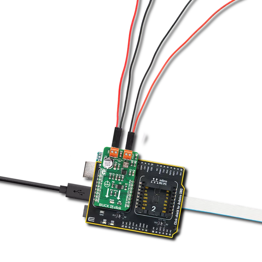
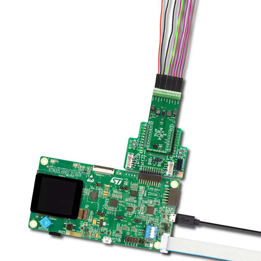
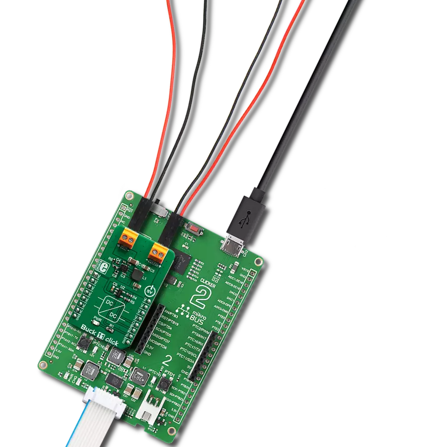
Start by selecting your development board and Click board™. Begin with the PIC32MZ clicker as your development board.


Software Support
Library Description
This library contains API for 3xBuck Click driver.
Key functions:
c3xbuck_enable_buck- This function enables desired Buck on the boardc3xbuck_disable_buck- This function disables desired Buck on the boardc3xbuck_set_voltage- This function sets voltage on desired Buck on the board
Open Source
Code example
The complete application code and a ready-to-use project are available through the NECTO Studio Package Manager for direct installation in the NECTO Studio. The application code can also be found on the MIKROE GitHub account.
/*!
 * \file
 * \brief 3xBuck Click example
 *
 * # Description
 * This example demonstrates the use of the 3 x Buck Click Board.
 *
 * The demo application is composed of two sections :
 *
 * ## Application Init
 * Initializes the driver and performs the Click default configuration.
 *
 * ## Application Task
 * Alternates between predefined and default values for the Bucks output and
 * logs the current set values on the USB UART.
 *
 * @note
 * The default output voltage on Buck 1 is 1800mV, Buck 2 is 3300mV, and Buck 3 is 5000mV.
 * Configurable output voltage on all Bucks ranges from 680mV to 1950mV.
 *
 * \author Petar Suknjaja
 *
 */
// ------------------------------------------------------------------- INCLUDES

#include "board.h"
#include "log.h"
#include "c3xbuck.h"

// ------------------------------------------------------------------ VARIABLES

static c3xbuck_t c3xbuck;
static log_t logger;

// ------------------------------------------------------ APPLICATION FUNCTIONS

void application_init ( void )
{
    log_cfg_t log_cfg;
    c3xbuck_cfg_t cfg;

    /**
     * Logger initialization.
     * Default baud rate: 115200
     * Default log level: LOG_LEVEL_DEBUG
     * @note If USB_UART_RX and USB_UART_TX
     * are defined as HAL_PIN_NC, you will
     * need to define them manually for log to work.
     * See @b LOG_MAP_USB_UART macro definition for detailed explanation.
     */
    LOG_MAP_USB_UART( log_cfg );
    log_init( &logger, &log_cfg );
    log_info( &logger, "---- Application Init ----" );

    //  Click initialization.

    c3xbuck_cfg_setup( &cfg );
    C3XBUCK_MAP_MIKROBUS( cfg, MIKROBUS_1 );
    c3xbuck_init( &c3xbuck, &cfg );
    Delay_ms ( 100 );

    c3xbuck_default_cfg ( &c3xbuck );
    log_info( &logger, "---- Application Task ----" );
}

void application_task ( void )
{
    //  Task implementation.
    log_printf( &logger, "Setting predefined values : \r\n" );
    log_printf( &logger, "Buck 1 : 1000 mV\r\n");
    log_printf( &logger, "Buck 2 : 1250 mV\r\n");
    log_printf( &logger, "Buck 3 : 1500 mV\r\n");

    c3xbuck_set_voltage( &c3xbuck, C3XBUCK_SELECT_BUCK_1, C3XBUCK_OUTPUT_VOLTAGE_1000mV );
    c3xbuck_set_voltage( &c3xbuck, C3XBUCK_SELECT_BUCK_2, C3XBUCK_OUTPUT_VOLTAGE_1250mV );
    c3xbuck_set_voltage( &c3xbuck, C3XBUCK_SELECT_BUCK_3, C3XBUCK_OUTPUT_VOLTAGE_1500mV );

    // 10 seconds delay
    Delay_ms ( 1000 );
    Delay_ms ( 1000 );
    Delay_ms ( 1000 );
    Delay_ms ( 1000 );
    Delay_ms ( 1000 );
    Delay_ms ( 1000 );
    Delay_ms ( 1000 );
    Delay_ms ( 1000 );
    Delay_ms ( 1000 );
    Delay_ms ( 1000 );

    log_printf( &logger, "Setting default values: \r\n");
    log_printf( &logger, "Buck 1 : 1800 mV\r\n");
    log_printf( &logger, "Buck 2 : 3300 mV\r\n");
    log_printf( &logger, "Buck 3 : 5000 mV\r\n");

    c3xbuck_set_voltage( &c3xbuck, C3XBUCK_SELECT_BUCK_1, C3XBUCK_BUCK_DEFAULT_OUTPUT_VOLTAGE );
    c3xbuck_set_voltage( &c3xbuck, C3XBUCK_SELECT_BUCK_2, C3XBUCK_BUCK_DEFAULT_OUTPUT_VOLTAGE );
    c3xbuck_set_voltage( &c3xbuck, C3XBUCK_SELECT_BUCK_3, C3XBUCK_BUCK_DEFAULT_OUTPUT_VOLTAGE );

    Delay_ms ( 1000 );
    Delay_ms ( 1000 );
    Delay_ms ( 1000 );
    Delay_ms ( 1000 );
    Delay_ms ( 1000 );
}

int main ( void )
{
    /* Do not remove this line or clock might not be set correctly. */
    #ifdef PREINIT_SUPPORTED
    preinit();
    #endif

    application_init( );

    for ( ; ; )
    {
        application_task( );
    }

    return 0;
}

// ------------------------------------------------------------------------ END