Monitor and respond to changes in the magnetic environment with US2882 and MK64FN1M0VDC12
Add a bipolar hall switch for smoother operations

Published Jun 20, 2023
Click board™
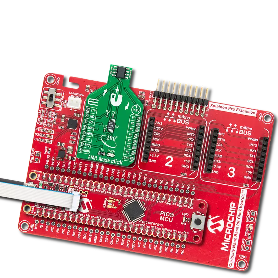
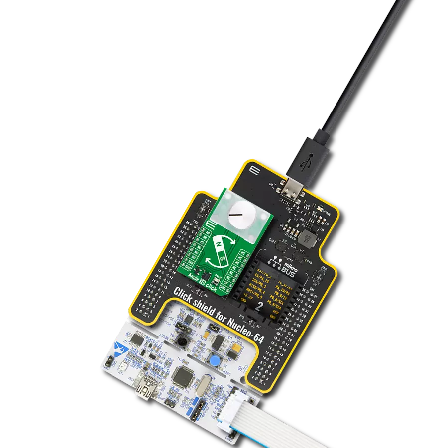
Bi Hall Click
Dev. board
Clicker 2 for Kinetis
Compiler
NECTO Studio
MCU
MK64FN1M0VDC12
By incorporating a bipolar Hall switch solution, you can ensure seamless switching between different states or modes in your design, enhancing its functionality and versatility
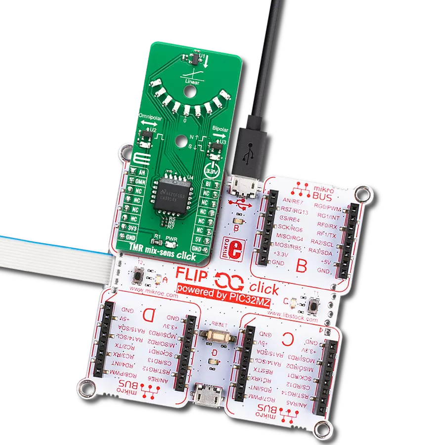
A
A
Hardware Overview
How does it work?
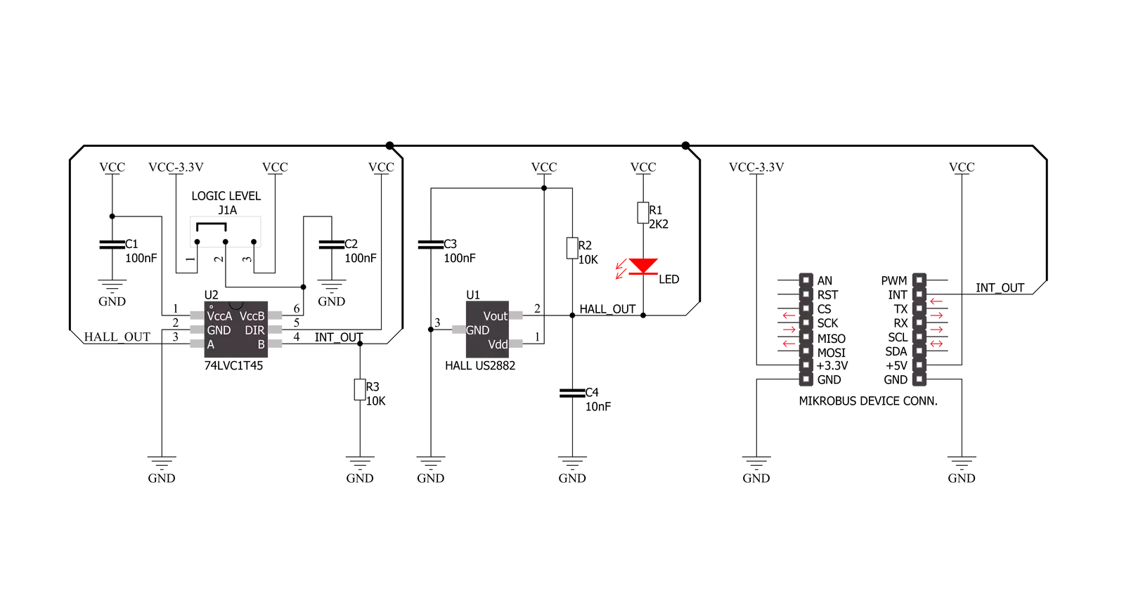
BI HALL Click is based on the US2882, a bipolar Hall-effect switch designed in mixed signal CMOS technology from Melexis Technologies. The US2882 comes with very high magnetic sensitivity based on mixed-signal CMOS technology. The US2882 integrates a voltage regulator, a Hall sensor with a dynamic offset cancellation system, a Schmitt trigger, and an open-drain output driver, all in a single package. It allows using generic magnets, weak magnets, or more significant air gaps, making it suitable for various automotive, consumer, and BLDC motor applications. The US2882 exhibits bipolar magnetic switching characteristics. Therefore, it operates with both the South and North poles. Typically, the device
behaves as a latch with symmetric operating and release switching points, which means magnetic fields with equivalent strength and opposite directions drive the output HIGH and LOW. In this way, it is possible to determine the pole of the magnet using the information that the host MCU receives from the sensor via the INT line of the mikroBUS™ socket. It is also possible to visually identify the magnet's North Pole via an onboard red LED. Removing the magnetic field keeps the output in its previous state, which defines the US2882 as a magnetic memory. Depending on the magnetic switching points, the US2882 may also behave as a unipolar positive or negative switch, which means the output can be set to HIGH and LOW by only
using one magnetic pole. In such a case, removing the magnetic field changes the output level. The chopper-stabilized amplifier uses a switched-capacitor technique to suppress the offset generally observed with Hall sensors and amplifiers. The CMOS technology makes this advanced technique possible, resulting in more stable magnetic characteristics. This Click board™ can operate with either 3.3V or 5V logic voltage levels selected via the LOGIC LEVEL jumper. This way, both 3.3V and 5V capable MCUs can use the communication lines properly. However, the Click board™ comes equipped with a library containing easy-to-use functions and an example code that can be used, as a reference, for further development.

Features overview
Development board
Clicker 2 for Kinetis is a compact starter development board that brings the flexibility of add-on Click boards™ to your favorite microcontroller, making it a perfect starter kit for implementing your ideas. It comes with an onboard 32-bit ARM Cortex-M4F microcontroller, the MK64FN1M0VDC12 from NXP Semiconductors, two mikroBUS™ sockets for Click board™ connectivity, a USB connector, LED indicators, buttons, a JTAG programmer connector, and two 26-pin headers for interfacing with external electronics. Its compact design with clear and easily recognizable silkscreen markings allows you to build gadgets with unique functionalities and
features quickly. Each part of the Clicker 2 for Kinetis development kit contains the components necessary for the most efficient operation of the same board. In addition to the possibility of choosing the Clicker 2 for Kinetis programming method, using a USB HID mikroBootloader or an external mikroProg connector for Kinetis programmer, the Clicker 2 board also includes a clean and regulated power supply module for the development kit. It provides two ways of board-powering; through the USB Micro-B cable, where onboard voltage regulators provide the appropriate voltage levels to each component on the board, or
using a Li-Polymer battery via an onboard battery connector. All communication methods that mikroBUS™ itself supports are on this board, including the well-established mikroBUS™ socket, reset button, and several user-configurable buttons and LED indicators. Clicker 2 for Kinetis is an integral part of the Mikroe ecosystem, allowing you to create a new application in minutes. Natively supported by Mikroe software tools, it covers many aspects of prototyping thanks to a considerable number of different Click boards™ (over a thousand boards), the number of which is growing every day.

Microcontroller Overview
MCU Card / MCU

Architecture
ARM Cortex-M4
MCU Memory (KB)
1024
Silicon Vendor
NXP
Pin count
121
RAM (Bytes)
262144
Used MCU Pins
mikroBUS™ mapper
Take a closer look
Click board™ Schematic
Step by step
Project assembly

Start by selecting your development board and Click board™. Begin with the Clicker 2 for Kinetis as your development board.


Track your results in real time
Application Output
1. Application Output - In Debug mode, the 'Application Output' window enables real-time data monitoring, offering direct insight into execution results. Ensure proper data display by configuring the environment correctly using the provided tutorial.

2. UART Terminal - Use the UART Terminal to monitor data transmission via a USB to UART converter, allowing direct communication between the Click board™ and your development system. Configure the baud rate and other serial settings according to your project's requirements to ensure proper functionality. For step-by-step setup instructions, refer to the provided tutorial.

3. Plot Output - The Plot feature offers a powerful way to visualize real-time sensor data, enabling trend analysis, debugging, and comparison of multiple data points. To set it up correctly, follow the provided tutorial, which includes a step-by-step example of using the Plot feature to display Click board™ readings. To use the Plot feature in your code, use the function: plot(*insert_graph_name*, variable_name);. This is a general format, and it is up to the user to replace 'insert_graph_name' with the actual graph name and 'variable_name' with the parameter to be displayed.

Software Support
Library Description
This library contains API for BI HALL Click driver.
Key functions:
bihall_det_mag_field- Detecting south and north pole magnetic fields status function
Open Source
Code example
The complete application code and a ready-to-use project are available through the NECTO Studio Package Manager for direct installation in the NECTO Studio. The application code can also be found on the MIKROE GitHub account.
/*!
 * \file
 * \brief BI HALL Click example
 *
 * # Description
 * Detect the south & north pole magnetic fields.
 *
 * The demo application is composed of two sections :
 *
 * ## Application Init
 * Configuring Clicks and log objects.
 *
 * ## Application Task
 * This is a example which demonstrates the use of BI HALL Click board.
 * Detect the south & north pole magnetic fields near the BI HALL Click.
 * Results are being sent to the Usart Terminal where you can track their changes.
 * All data logs on usb uart when magnetic field is detected.
 *
 * \author Nenad Filipovic
 *
 */
// ------------------------------------------------------------------- INCLUDES

#include "board.h"
#include "log.h"
#include "bihall.h"

// ------------------------------------------------------------------ VARIABLES

static bihall_t bihall;
static log_t logger;

uint8_t bihall_state;
uint8_t bihall_state_old;

// ------------------------------------------------------- ADDITIONAL FUNCTIONS


// ------------------------------------------------------ APPLICATION FUNCTIONS

void application_init ( void )
{
    log_cfg_t log_cfg;
    bihall_cfg_t cfg;

    /**
     * Logger initialization.
     * Default baud rate: 115200
     * Default log level: LOG_LEVEL_DEBUG
     * @note If USB_UART_RX and USB_UART_TX
     * are defined as HAL_PIN_NC, you will
     * need to define them manually for log to work.
     * See @b LOG_MAP_USB_UART macro definition for detailed explanation.
     */
    LOG_MAP_USB_UART( log_cfg );
    log_init( &logger, &log_cfg );
    log_printf(&logger, "---- Application Init ----\r\n");

    //  Click initialization.

    bihall_cfg_setup( &cfg );
    BIHALL_MAP_MIKROBUS( cfg, MIKROBUS_1 );
    bihall_init( &bihall, &cfg );

    log_printf(&logger, " Detecting magnetic fields\r\n");
    log_printf(&logger, "--------------------------\r\n");

    bihall_state = BIHALL_MAG_POLE_NORTH;
    bihall_state_old = BIHALL_MAG_POLE_NORTH;
}

void application_task ( void )
{
    bihall_state = bihall_det_mag_field( &bihall );

    if ( ( bihall_state == BIHALL_MAG_POLE_SOUTH ) && ( bihall_state_old == BIHALL_MAG_POLE_NORTH ) )
    {
        bihall_state_old = BIHALL_MAG_POLE_SOUTH;
        log_printf(&logger, "         ~ SOUTH ~\r\n");
        log_printf(&logger, "--------------------------\r\n");
    }

    if ( ( bihall_state == BIHALL_MAG_POLE_NORTH ) && ( bihall_state_old == BIHALL_MAG_POLE_SOUTH ) )
    {
        log_printf(&logger, "         ~ NORTH ~\r\n");
        log_printf(&logger, "--------------------------\r\n");
        bihall_state_old = BIHALL_MAG_POLE_NORTH;
    }
}

int main ( void )
{
    /* Do not remove this line or clock might not be set correctly. */
    #ifdef PREINIT_SUPPORTED
    preinit();
    #endif

    application_init( );

    for ( ; ; )
    {
        application_task( );
    }

    return 0;
}


// ------------------------------------------------------------------------ END