Transform voltage like never before with MPM3530 and STM32L041C6
Sync your power needs

Published Aug 01, 2023
Click board™
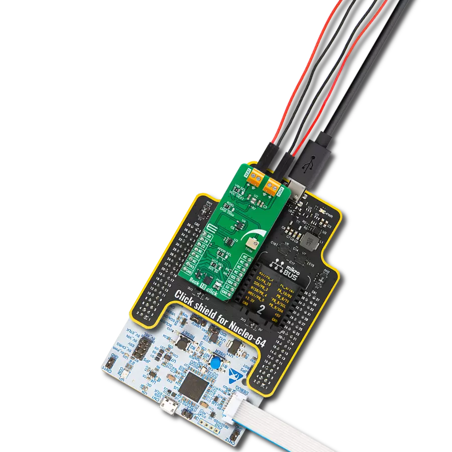
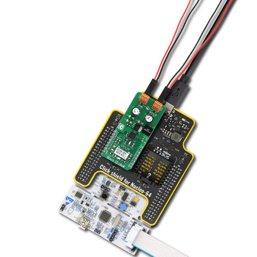
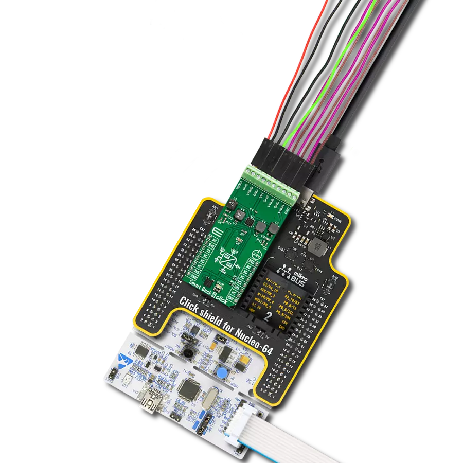
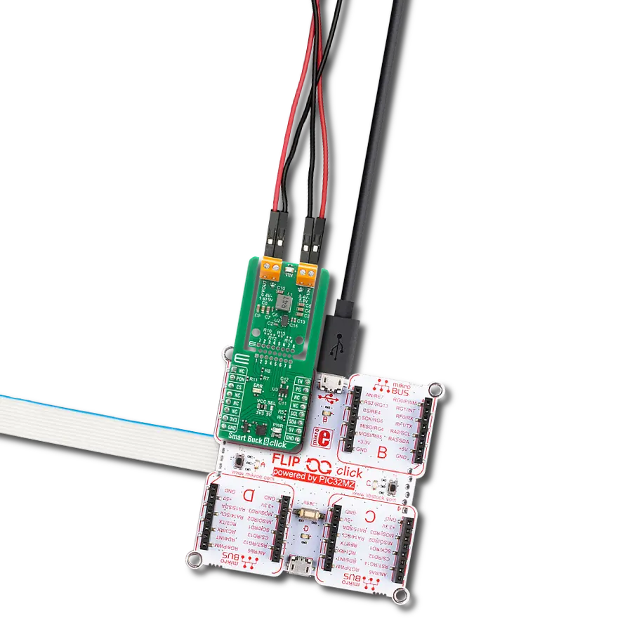
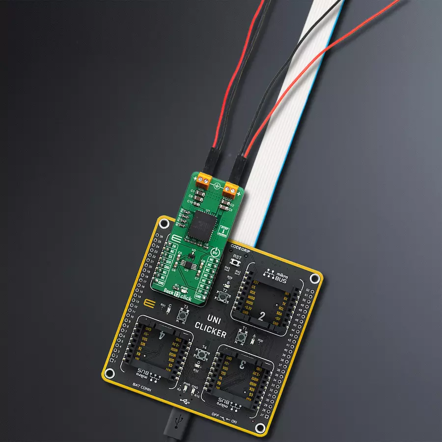
Buck 13 Click
Dev. board
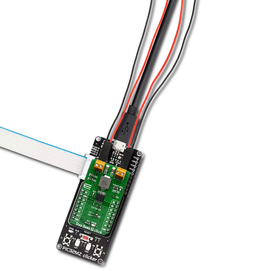
UNI Clicker
Compiler
NECTO Studio
MCU
STM32L041C6
Ensure your electronics receive the necessary power, minimizing waste and enhancing performance
A
A
Hardware Overview
How does it work?
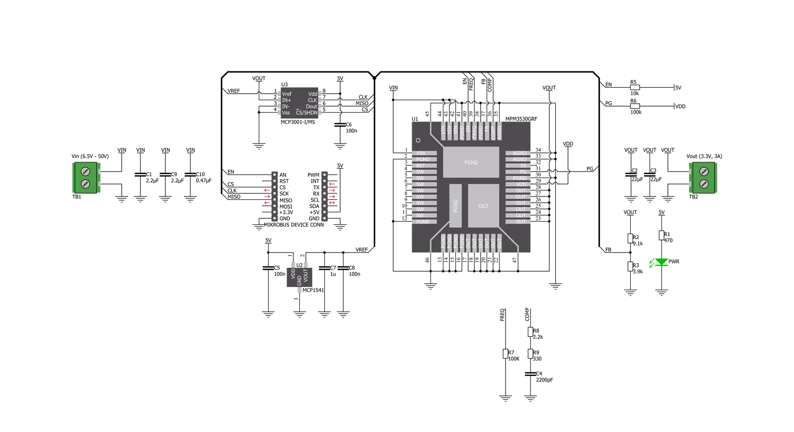
Buck 13 Click is based on the MPM3530, a 55V 3A ultra-low profile DC-to-DC power module by Monolithic Power Systems (MPS). This IC is a valley current mode controlled power module, meaning that it responds faster than the traditional peak current mode control, thus, a better response to transients. This IC requires minimal external components, making the whole device robust and easy to work with. The feedback voltage on the FB pin determines the output voltage. Therefore, Buck 13 click has a fixed voltage divider calculated to ensure stable, the most frequently used, 3.3V output. The MPM3530 operates at a high switching frequency of 520 kHz, which allows a good compromise between the efficiency and the device's size, with no external coil needed and a minimal number of other external components. This Click board™ also uses the MCP3001, a 10-bit A/D converter (ADC) which uses the SPI interface from Microchip. It allows monitoring of the
output voltage over the SPI interface. This ADC is powered by the +5V mikroBUS™ power rail. The same voltage is also used to supply the MCP1541 voltage reference. That way, the stable 4.096V reference voltage is obtained to ensure precise output voltage measurement. The Click board™ itself requires an external power supply to be connected at the input terminal, labeled as VIN. The VOUT terminal provides the connected load with the regulated 3.3V voltage. The over-current protection is based on cycle-by-cycle limiting of the inductor current. If the output voltage starts to drop during the current limiting interval, causing the FB voltage to drop under 50% of the internal reference, the device enters the hiccup mode, shutting down the output. After a fixed period, the device will try to re-enable the output. If the short-circuit condition still exists, it will shut down the output again, repeating the whole process until the short-circuit condition disappears. The hiccup
mode greatly reduces the short-circuit current, protecting the device when the output is shorted to ground. Thanks to its ability to work with the high-duty cycle of the internal switching PWM signal, the MPM3530 requires the input voltage to be only about 0.7V above the output voltage to maintain the regulation. However, if the input voltage drops under 3.5V, the device cannot operate properly. Therefore, the under-voltage protection shuts down the device as a protection measure. The under-voltage protection is disabled once the input voltage exceeds 3.9V. This small hysteresis of 0.4V prevents erratic behavior in border cases. As mentioned before, the voltage of the power supply at the input terminal should stay within the range between 4V and 55V. However, the voltage at the input should be approximately 5.7V to 6V, at least, to provide good regulation at the output.

Features overview
Development board
UNI Clicker is a compact development board designed as a complete solution that brings the flexibility of add-on Click boards™ to your favorite microcontroller, making it a perfect starter kit for implementing your ideas. It supports a wide range of microcontrollers, such as different ARM, PIC32, dsPIC, PIC, and AVR from various vendors like Microchip, ST, NXP, and TI (regardless of their number of pins), four mikroBUS™ sockets for Click board™ connectivity, a USB connector, LED indicators, buttons, a debugger/programmer connector, and two 26-pin headers for interfacing with external electronics. Thanks to innovative manufacturing technology, it allows you to build
gadgets with unique functionalities and features quickly. Each part of the UNI Clicker development kit contains the components necessary for the most efficient operation of the same board. In addition to the possibility of choosing the UNI Clicker programming method, using a third-party programmer or CODEGRIP/mikroProg connected to onboard JTAG/SWD header, the UNI Clicker board also includes a clean and regulated power supply module for the development kit. It provides two ways of board-powering; through the USB Type-C (USB-C) connector, where onboard voltage regulators provide the appropriate voltage levels to each component on the board, or using a Li-Po/Li
Ion battery via an onboard battery connector. All communication methods that mikroBUS™ itself supports are on this board (plus USB HOST/DEVICE), including the well-established mikroBUS™ socket, a standardized socket for the MCU card (SiBRAIN standard), and several user-configurable buttons and LED indicators. UNI Clicker is an integral part of the Mikroe ecosystem, allowing you to create a new application in minutes. Natively supported by Mikroe software tools, it covers many aspects of prototyping thanks to a considerable number of different Click boards™ (over a thousand boards), the number of which is growing every day.

Microcontroller Overview
MCU Card / MCU
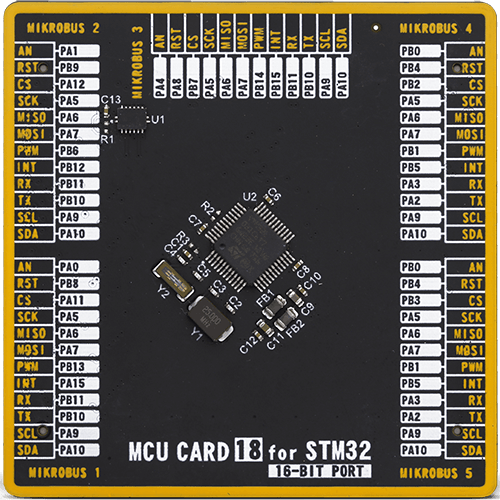
Type
8th Generation
Architecture
ARM Cortex-M0
MCU Memory (KB)
32
Silicon Vendor
STMicroelectronics
Pin count
48
RAM (Bytes)
8192
Used MCU Pins
mikroBUS™ mapper
Take a closer look
Click board™ Schematic
Step by step
Project assembly

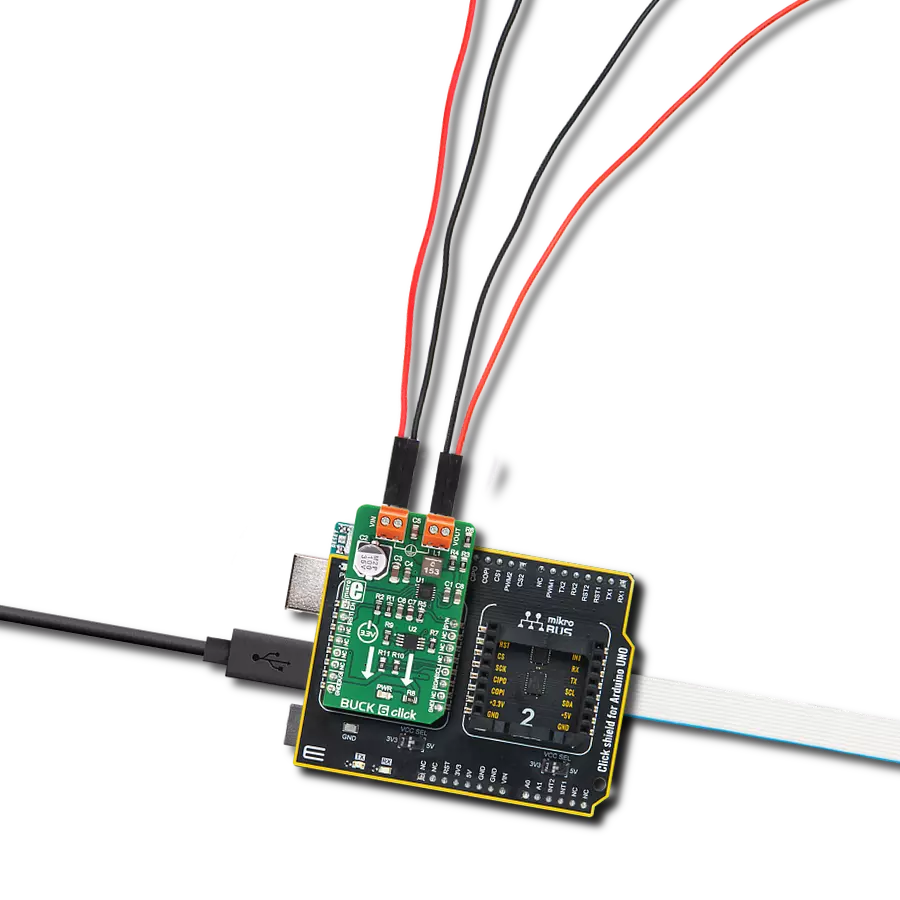
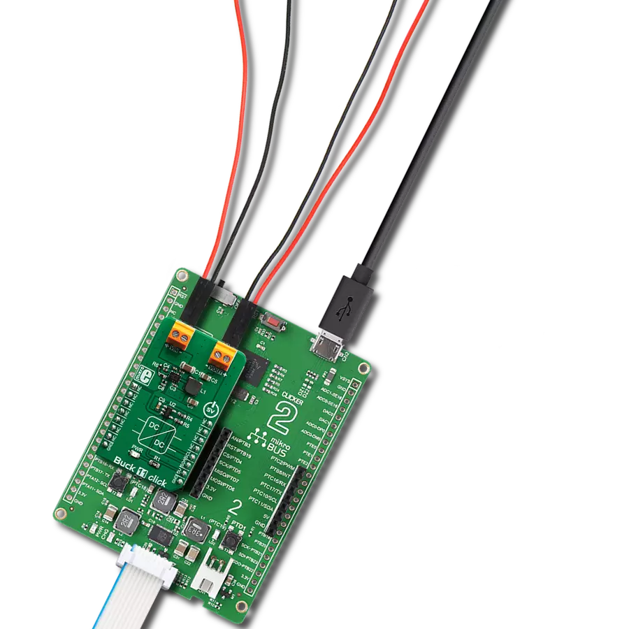
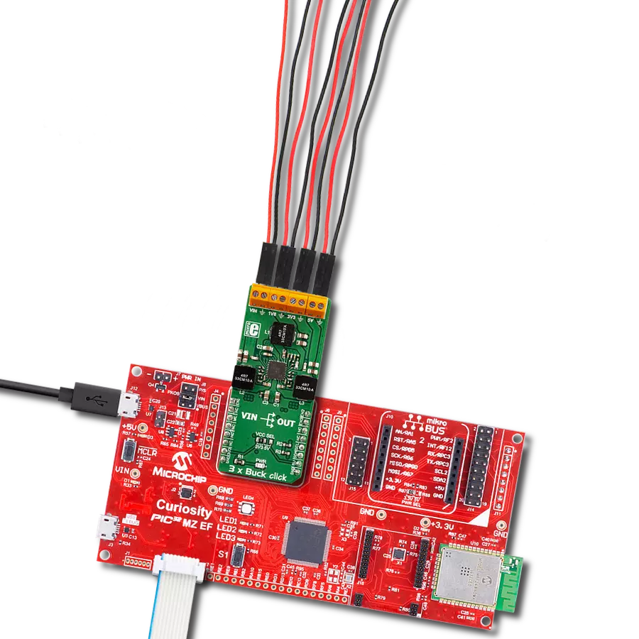
Start by selecting your development board and Click board™. Begin with the UNI Clicker as your development board.


Software Support
Library Description
This library contains API for Buck 13 Click driver.
Key functions:
buck13_enable- Enables the Buck 13 outputbuck13_get_adc- Gets the ADC values from the modulebuck13_get_voltage- Gets the output voltage
Open Source
Code example
The complete application code and a ready-to-use project are available through the NECTO Studio Package Manager for direct installation in the NECTO Studio. The application code can also be found on the MIKROE GitHub account.
/*!
 * \file
 * \brief Buck13 Click example
 *
 * # Description
 * This example switches the output of the Buck13 and logs the output voltage
 * on the Vout terminal.
 *
 * The demo application is composed of two sections :
 *
 * ## Application Init
 * Initializes SPI serial interface and turns OFF the Buck 13 output as default state.
 *
 * ## Application Task
 * Displays the output voltage every 2 seconds.
 *
 * *note:*
 * Input voltage range must be from 6.5 to 50V.
 * Output voltage is about 3.3V.
 * Current limit is 3A.
 *
 * \author Petar Suknjaja
 *
 */
// ------------------------------------------------------------------- INCLUDES

#include "board.h"
#include "log.h"
#include "buck13.h"

// ------------------------------------------------------------------ VARIABLES

static buck13_t buck13;
static log_t logger;
static uint16_t out_voltage;

// ------------------------------------------------------ APPLICATION FUNCTIONS

void application_init ( void )
{
    log_cfg_t log_cfg;
    buck13_cfg_t cfg;

    /**
     * Logger initialization.
     * Default baud rate: 115200
     * Default log level: LOG_LEVEL_DEBUG
     * @note If USB_UART_RX and USB_UART_TX
     * are defined as HAL_PIN_NC, you will
     * need to define them manually for log to work.
     * See @b LOG_MAP_USB_UART macro definition for detailed explanation.
     */
    LOG_MAP_USB_UART( log_cfg );
    log_init( &logger, &log_cfg );
    log_info( &logger, "---- Application Init ----" );

    //  Click initialization.

    buck13_cfg_setup( &cfg );
    BUCK13_MAP_MIKROBUS( cfg, MIKROBUS_1 );
    buck13_default_cfg ( &buck13 );
    buck13_init( &buck13, &cfg );
    log_info( &logger, "Buck 13 is enabled now" );
}

void application_task ( void )
{
    //  Task implementation.

    buck13_enable( &buck13, BUCK13_ENABLE );
    out_voltage = buck13_get_voltage( &buck13 );
    log_printf( &logger, "Vout =  %d mV\r\n", out_voltage );

    Delay_ms ( 1000 );
    Delay_ms ( 1000 );
}

int main ( void )
{
    /* Do not remove this line or clock might not be set correctly. */
    #ifdef PREINIT_SUPPORTED
    preinit();
    #endif

    application_init( );

    for ( ; ; )
    {
        application_task( );
    }

    return 0;
}

// ------------------------------------------------------------------------ END