Ensure stable and safe operation of various systems with MIC33153 and PIC18F57Q43
Convert voltage with confidence!

Published Feb 13, 2024
Click board™
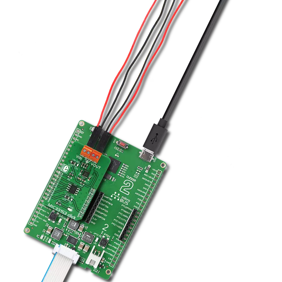
MIC33153 Click
Dev. board
Curiosity Nano with PIC18F57Q43
Compiler
NECTO Studio
MCU
PIC18F57Q43
Upgrade to a more efficient voltage solution, integrate DC-DC buck regulator, power up applications with clean voltage!
A
A
Hardware Overview
How does it work?
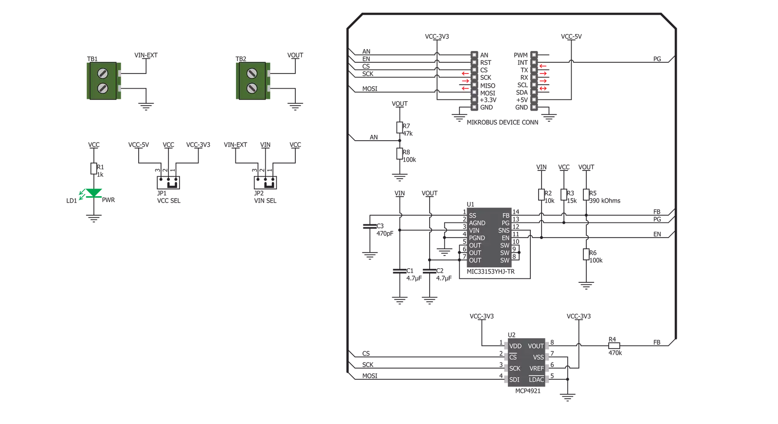
MIC33153 Click is based on the MIC33153, a 4MHz DC-DC buck regulator with integrated inductor and Hyperlight Load™ technology, from Microchip. This integrated buck regulator requires minimal external components, including the inductor. This simplifies the design greatly, retaining the advertised electrical characteristics. Also, thermal shutdown and current limit protection features ensure safe operation, even in case of errors and short circuits. This Click operates with an input voltage range from 2.7V up to 5.5V, and it can deliver a regulated output ranging from 0.8V to 3.5V, with up to 1.2A. The output voltage is selectable, and the voltage on the FB pin manages it. This pin is routed to the output of the MCP4921, a 12-bit DAC converter from Microchip, with the SPI interface. The voltage on the DAC output affects the FB pin voltage, which in turn affects the main output voltage. A voltage divider connected between the main output terminal and the GND allows monitoring of the output voltage via the AN pin of the mikroBUS™. This gives an insight into the output voltage condition: if the output voltage deviates from the desired value, the corrected value can be sent to the DAC. MCP4921 DAC converter has its SPI lines routed to the mikroBUS™, so it is enough to send a new value via the SPI of the click board™ if a correction is needed. Of course, being a buck converter,
the Click board™ expects higher input voltage than it is set at its output. The proprietary HyperLight Load™ technology allows it to operate efficiently when a very light load is connected to the output terminal. Instead of using the continuous PWM signal to operate the DC-DC buck converter, it goes into the discontinuous mode, with the pulse frequency modulation (PFM) signal used for regulating the output. As the output current rises, the device enters the continuous conducting mode (CCM) with the PWM frequency at 4MHz. The transition is transparent and happens automatically when the output current rises above a certain level. This level depends on the duty cycle of the internal PWM signal, input and output voltages, PWM frequency, and the internal coil inductance, and it is about 200mA for the VIN = 3.6V and VOUT = 1.8V. The EN pin of the MIC33153 is also routed to the mikroBUS™, and it is used to turn off the output stage of the DC-DC step-down converter. A logic HIGH signal will activate the device, while the logic LOW will put the device in shutdown mode with very low power consumption. The EN pin is subject to a soft start circuitry that reduces the inrush current and prevents the output voltage from overshooting at the start-up. The Soft start delay is determined by the capacitor connected to the SS pin, which is fixed to around 300µS for the
MIC33153 Click. The EN pin is pulled HIGH by the onboard resistor. The PG pin of the MIC33153 is routed to the INT pin of the mikroBUS™, and it is used to signalize the power good status of the output voltage. An open drain output is pulled low when the output voltage drops under 86%. It reverts to the HIGH logic state when the output voltage reaches 92% of its steady state. It can generate the interrupt event on the controller or otherwise signal the output voltage problem. The PG pin is pulled HIGH by the onboard resistor. The MIC33153 click has two robust screw terminals connecting the input and output voltage rails. Instead of the input terminal, the click can use the voltage input from the development system if the VIN SEL SMD jumper is switched to the VCC position (default jumper position). MIC33153 click can work with both 3.3V and 5V rated MCUs. The VCC SEL SMD jumper should be switched to the correct position, indicated by the label - 3.3V or 5V, to select the desired operational voltage. It should be noted that the selected voltage will be used as the internal voltage supply for the buck converter input if selected so by the VIN SEL. Also, 3.3V is required regardless of the position of the VCC SEL jumper since the MCP4921 DAC is powered up from the 3.3V rail directly.

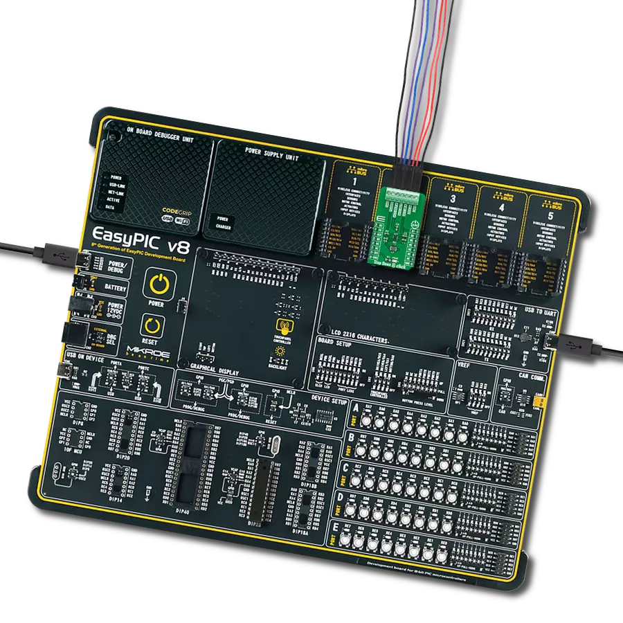
Features overview
Development board
PIC18F57Q43 Curiosity Nano evaluation kit is a cutting-edge hardware platform designed to evaluate microcontrollers within the PIC18-Q43 family. Central to its design is the inclusion of the powerful PIC18F57Q43 microcontroller (MCU), offering advanced functionalities and robust performance. Key features of this evaluation kit include a yellow user LED and a responsive
mechanical user switch, providing seamless interaction and testing. The provision for a 32.768kHz crystal footprint ensures precision timing capabilities. With an onboard debugger boasting a green power and status LED, programming and debugging become intuitive and efficient. Further enhancing its utility is the Virtual serial port (CDC) and a debug GPIO channel (DGI
GPIO), offering extensive connectivity options. Powered via USB, this kit boasts an adjustable target voltage feature facilitated by the MIC5353 LDO regulator, ensuring stable operation with an output voltage ranging from 1.8V to 5.1V, with a maximum output current of 500mA, subject to ambient temperature and voltage constraints.

Microcontroller Overview
MCU Card / MCU

Architecture
PIC
MCU Memory (KB)
128
Silicon Vendor
Microchip
Pin count
48
RAM (Bytes)
8196
You complete me!
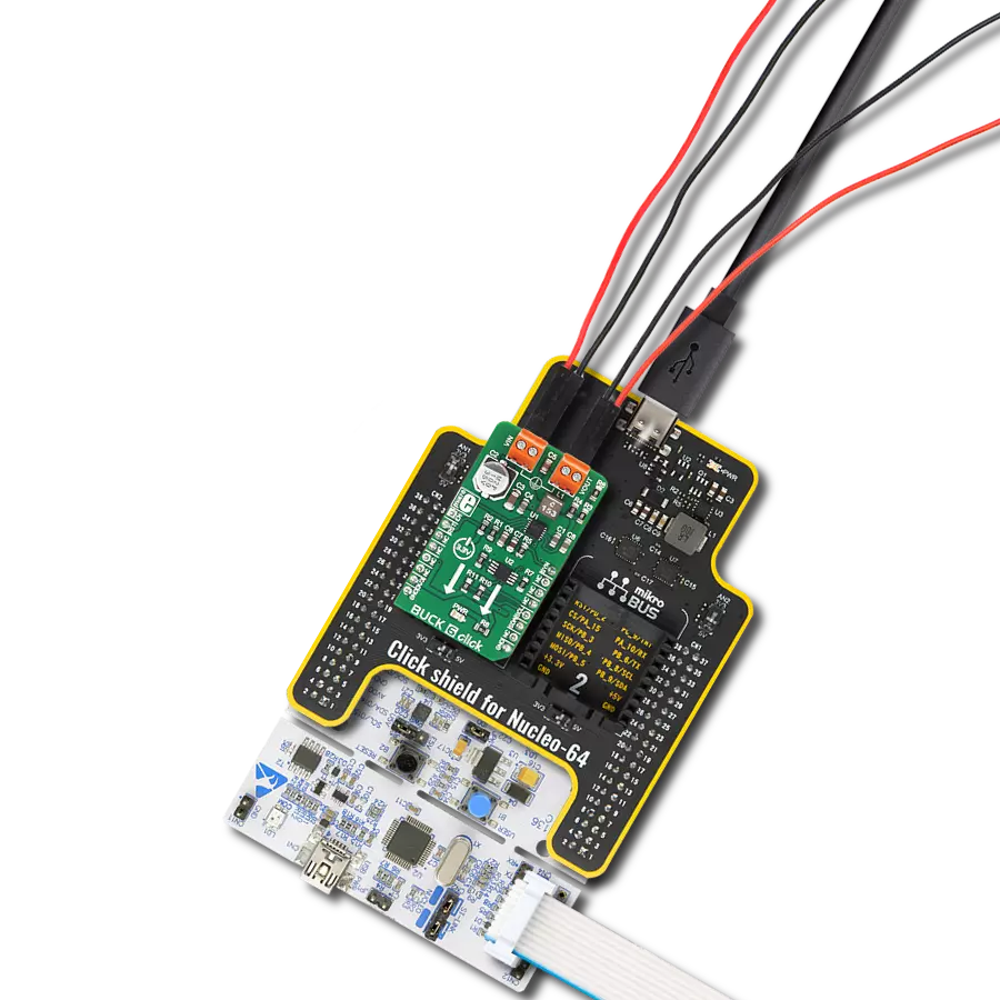
Accessories
Curiosity Nano Base for Click boards is a versatile hardware extension platform created to streamline the integration between Curiosity Nano kits and extension boards, tailored explicitly for the mikroBUS™-standardized Click boards and Xplained Pro extension boards. This innovative base board (shield) offers seamless connectivity and expansion possibilities, simplifying experimentation and development. Key features include USB power compatibility from the Curiosity Nano kit, alongside an alternative external power input option for enhanced flexibility. The onboard Li-Ion/LiPo charger and management circuit ensure smooth operation for battery-powered applications, simplifying usage and management. Moreover, the base incorporates a fixed 3.3V PSU dedicated to target and mikroBUS™ power rails, alongside a fixed 5.0V boost converter catering to 5V power rails of mikroBUS™ sockets, providing stable power delivery for various connected devices.

Used MCU Pins
mikroBUS™ mapper
Take a closer look
Click board™ Schematic
Step by step
Project assembly

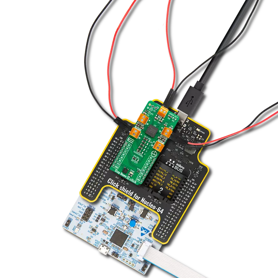
Start by selecting your development board and Click board™. Begin with the Curiosity Nano with PIC18F57Q43 as your development board.


Track your results in real time
Application Output
1. Application Output - In Debug mode, the 'Application Output' window enables real-time data monitoring, offering direct insight into execution results. Ensure proper data display by configuring the environment correctly using the provided tutorial.

2. UART Terminal - Use the UART Terminal to monitor data transmission via a USB to UART converter, allowing direct communication between the Click board™ and your development system. Configure the baud rate and other serial settings according to your project's requirements to ensure proper functionality. For step-by-step setup instructions, refer to the provided tutorial.

3. Plot Output - The Plot feature offers a powerful way to visualize real-time sensor data, enabling trend analysis, debugging, and comparison of multiple data points. To set it up correctly, follow the provided tutorial, which includes a step-by-step example of using the Plot feature to display Click board™ readings. To use the Plot feature in your code, use the function: plot(*insert_graph_name*, variable_name);. This is a general format, and it is up to the user to replace 'insert_graph_name' with the actual graph name and 'variable_name' with the parameter to be displayed.

Software Support
Library Description
This library contains API for MIC33153 Click driver.
Key functions:
mic33153_write_dac- This function writes 12-bit value to DAC and that causes that output voltage be seted on determined valuemic33153_enable_out- This function enables or disables output voltage depending on the state valuemic33153_check_power_good- This function hecks state of PG (INT) pin
Open Source
Code example
The complete application code and a ready-to-use project are available through the NECTO Studio Package Manager for direct installation in the NECTO Studio. The application code can also be found on the MIKROE GitHub account.
/*!
 * \file
 * \brief Mic33153 Click example
 *
 * # Description
 * This app enables step-down (buck) converter.
 *
 * The demo application is composed of two sections :
 *
 * ## Application Init
 * Initializes Click driver.
 *
 * ## Application Task
 * Activates the output voltage of the device, and then sets output voltage to various different values.
 * All data is being logged on USB UART.
 *
 * \author MikroE Team
 *
 */
// ------------------------------------------------------------------- INCLUDES

#include "board.h"
#include "log.h"
#include "mic33153.h"

// ------------------------------------------------------------------ VARIABLES

static mic33153_t mic33153;
static log_t logger;

// ------------------------------------------------------ APPLICATION FUNCTIONS

void application_init ( void )
{
    log_cfg_t log_cfg;
    mic33153_cfg_t cfg;

    /**
     * Logger initialization.
     * Default baud rate: 115200
     * Default log level: LOG_LEVEL_DEBUG
     * @note If USB_UART_RX and USB_UART_TX
     * are defined as HAL_PIN_NC, you will
     * need to define them manually for log to work.
     * See @b LOG_MAP_USB_UART macro definition for detailed explanation.
     */
    LOG_MAP_USB_UART( log_cfg );
    log_init( &logger, &log_cfg );
    log_info( &logger, "---- Application Init ----" );

    //  Click initialization.

    mic33153_cfg_setup( &cfg );
    MIC33153_MAP_MIKROBUS( cfg, MIKROBUS_1 );
    mic33153_init( &mic33153, &cfg );
    Delay_ms ( 100 );
}

void application_task ( void )
{
    mic33153_enable_out( &mic33153, MIC33153_OUT_ENABLE );

    mic33153_write_dac ( &mic33153, MIC33153_VOLTAGE_1000MV );
    log_printf( &logger, "Output voltage set to 1000mV\r\n" );
    Delay_ms ( 1000 );
    Delay_ms ( 1000 );

    mic33153_write_dac ( &mic33153, MIC33153_VOLTAGE_1500MV );
    log_printf( &logger, "Output voltage set to 1500mV\r\n" );
    Delay_ms ( 1000 );
    Delay_ms ( 1000 );

    mic33153_write_dac ( &mic33153, MIC33153_VOLTAGE_2000MV );
    log_printf( &logger, "Output voltage set to 2000mV\r\n" );
    Delay_ms ( 1000 );
    Delay_ms ( 1000 );

    mic33153_write_dac ( &mic33153, MIC33153_VOLTAGE_2500MV );
    log_printf( &logger, "Output voltage set to 2500mV\r\n" );
    Delay_ms ( 1000 );
    Delay_ms ( 1000 );

    mic33153_write_dac ( &mic33153, MIC33153_VOLTAGE_3000MV );
    log_printf( &logger, "Output voltage set to 3000mV\r\n" );
    Delay_ms ( 1000 );
    Delay_ms ( 1000 );

    mic33153_write_dac ( &mic33153, MIC33153_VOLTAGE_3200MV );
    log_printf( &logger, "Output voltage set to 3200mV\r\n" );
    Delay_ms ( 1000 );
    Delay_ms ( 1000 );

    log_printf( &logger, "-----------------------------------\r\n" );
}

int main ( void )
{
    /* Do not remove this line or clock might not be set correctly. */
    #ifdef PREINIT_SUPPORTED
    preinit();
    #endif

    application_init( );

    for ( ; ; )
    {
        application_task( );
    }

    return 0;
}

// ------------------------------------------------------------------------ END
Additional Support
Resources
Category:Buck