Create a reliable and secure data storage and transfer with W25Q02JV and ATmega328P
Got memory? With flash memory, you do!

Published Feb 14, 2024
Click board™
Flash 9 Click
Dev. board
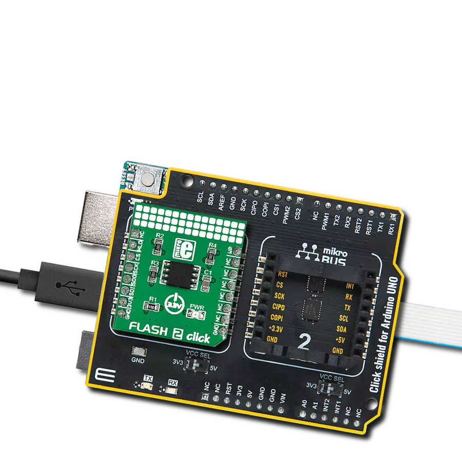
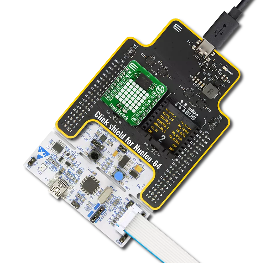
Arduino UNO Rev3
Compiler
NECTO Studio
MCU
ATmega328P
Discover a new level of memory performance and security with this SPI serial flash memory solution
A
A
Hardware Overview
How does it work?
Flash 9 Click is based on the W25Q02JV, a highly reliable serial Flash memory solution offering flexibility and performance well beyond ordinary Serial Flash devices from Winbond Electronics. The W25Q02JV represents a four 512Mb stack die where only one can be active at any given time to communicate with the external SPI controller. It supports linear addressing for the full 2Gb memory address range (continuously read accessible only into four separate 512Mb address memory segments). The W25Q02JV array is organized into 1,048,576 programmable pages of 256 bytes each, where up to 256 bytes can be programmed at a time. Pages of the W25Q02JV can be erased in groups of 16 (4KB sector erase), groups of 128 (32KB block erase), groups of 256 (64KB block erase), or the entire chip (chip erase). This IC has 32,768 erasable 4KB sectors and 2,048 erasable 64KB blocks, respectively.
The small 4KB sectors allow for greater flexibility in applications that require data and parameter storage. Also, it specifies a minimum of 100.000 endurance cycles with data retention of a minimum of 20 years, which gives the W25Q02JV the capability to handle unlimited reads/writes to the memory. Flash 9 Click communicates with MCU through a standard SPI interface that enables high clock speed, supporting the two most common SPI modes, SPI Mode 0 and 3. Alongside the internal software Reset sequence, this board has an active-low reset signal routed on the RST pin of the mikroBUS™ socket used to reset the W25Q02JV to the initial power-on state. When this signal is asserted low, any ongoing program/erase operation will be interrupted, and data corruption may happen (the device will not accept any command input). An additional feature of this Click board™
represents the configurable Write Protection function labeled as WP routed on the AN pin of the mikroBUS™ socket. The WP pin protects the entire memory and all registers from write operations and must be set to a low logic state to inhibit all the write operations. Besides, the Flash 9 Click also has an additional hold pin, labeled as HLD, and routed to the PWM pin of the mikroBUS™ socket, allowing the device to be paused while it’s still actively selected. This Click board™ can only be operated with a 3.3V logic voltage level. The board must perform appropriate logic voltage level conversion before using MCUs with different logic levels. However, the Click board™ comes equipped with a library containing functions and an example code that can be used as a reference for further development.


Features overview
Development board
Arduino UNO is a versatile microcontroller board built around the ATmega328P chip. It offers extensive connectivity options for various projects, featuring 14 digital input/output pins, six of which are PWM-capable, along with six analog inputs. Its core components include a 16MHz ceramic resonator, a USB connection, a power jack, an
ICSP header, and a reset button, providing everything necessary to power and program the board. The Uno is ready to go, whether connected to a computer via USB or powered by an AC-to-DC adapter or battery. As the first USB Arduino board, it serves as the benchmark for the Arduino platform, with "Uno" symbolizing its status as the
first in a series. This name choice, meaning "one" in Italian, commemorates the launch of Arduino Software (IDE) 1.0. Initially introduced alongside version 1.0 of the Arduino Software (IDE), the Uno has since become the foundational model for subsequent Arduino releases, embodying the platform's evolution.

Microcontroller Overview
MCU Card / MCU

Architecture
AVR
MCU Memory (KB)
32
Silicon Vendor
Microchip
Pin count
28
RAM (Bytes)
2048
You complete me!
Accessories
Click Shield for Arduino UNO has two proprietary mikroBUS™ sockets, allowing all the Click board™ devices to be interfaced with the Arduino UNO board without effort. The Arduino Uno, a microcontroller board based on the ATmega328P, provides an affordable and flexible way for users to try out new concepts and build prototypes with the ATmega328P microcontroller from various combinations of performance, power consumption, and features. The Arduino Uno has 14 digital input/output pins (of which six can be used as PWM outputs), six analog inputs, a 16 MHz ceramic resonator (CSTCE16M0V53-R0), a USB connection, a power jack, an ICSP header, and reset button. Most of the ATmega328P microcontroller pins are brought to the IO pins on the left and right edge of the board, which are then connected to two existing mikroBUS™ sockets. This Click Shield also has several switches that perform functions such as selecting the logic levels of analog signals on mikroBUS™ sockets and selecting logic voltage levels of the mikroBUS™ sockets themselves. Besides, the user is offered the possibility of using any Click board™ with the help of existing bidirectional level-shifting voltage translators, regardless of whether the Click board™ operates at a 3.3V or 5V logic voltage level. Once you connect the Arduino UNO board with our Click Shield for Arduino UNO, you can access hundreds of Click boards™, working with 3.3V or 5V logic voltage levels.

Used MCU Pins
mikroBUS™ mapper
Take a closer look
Click board™ Schematic

Step by step
Project assembly

Start by selecting your development board and Click board™. Begin with the Arduino UNO Rev3 as your development board.


Track your results in real time
Application Output
1. Application Output - In Debug mode, the 'Application Output' window enables real-time data monitoring, offering direct insight into execution results. Ensure proper data display by configuring the environment correctly using the provided tutorial.

2. UART Terminal - Use the UART Terminal to monitor data transmission via a USB to UART converter, allowing direct communication between the Click board™ and your development system. Configure the baud rate and other serial settings according to your project's requirements to ensure proper functionality. For step-by-step setup instructions, refer to the provided tutorial.

3. Plot Output - The Plot feature offers a powerful way to visualize real-time sensor data, enabling trend analysis, debugging, and comparison of multiple data points. To set it up correctly, follow the provided tutorial, which includes a step-by-step example of using the Plot feature to display Click board™ readings. To use the Plot feature in your code, use the function: plot(*insert_graph_name*, variable_name);. This is a general format, and it is up to the user to replace 'insert_graph_name' with the actual graph name and 'variable_name' with the parameter to be displayed.

Software Support
Library Description
This library contains API for Flash 9 Click driver.
Key functions:
flash9_erase_memoryThis function erases the selected amount of memory that contains the selected address.flash9_memory_writeThis function writes a desired number of data bytes to the memory starting from the selected address.flash9_memory_read_fastThis function reads a desired number of data bytes from memory starting from the selected address performing the fast read command.
Open Source
Code example
The complete application code and a ready-to-use project are available through the NECTO Studio Package Manager for direct installation in the NECTO Studio. The application code can also be found on the MIKROE GitHub account.
/*!
 * @file main.c
 * @brief Flash9 Click example
 *
 * # Description
 * This example demonstrates the use of Flash 9 Click board by writing specified data to
 * the memory and reading it back.
 *
 * The demo application is composed of two sections :
 *
 * ## Application Init
 * Initializes the driver and performs the Click default configuration.
 *
 * ## Application Task
 * Erases the memory sector and then writes a desired number of data bytes to the memory
 * and verifies that it is written correctly by reading from the same memory location and
 * displaying the memory content on the USB UART.
 *
 * @author Stefan Filipovic
 *
 */

#include "board.h"
#include "log.h"
#include "flash9.h"

#define DEMO_TEXT_MESSAGE           "MikroE - Flash 9 Click board"
#define STARTING_ADDRESS            0x01234567ul

static flash9_t flash9;
static log_t logger;

void application_init ( void )
{
    log_cfg_t log_cfg;  /**< Logger config object. */
    flash9_cfg_t flash9_cfg;  /**< Click config object. */

    /**
     * Logger initialization.
     * Default baud rate: 115200
     * Default log level: LOG_LEVEL_DEBUG
     * @note If USB_UART_RX and USB_UART_TX
     * are defined as HAL_PIN_NC, you will
     * need to define them manually for log to work.
     * See @b LOG_MAP_USB_UART macro definition for detailed explanation.
     */
    LOG_MAP_USB_UART( log_cfg );
    log_init( &logger, &log_cfg );
    log_info( &logger, " Application Init " );

    // Click initialization.
    flash9_cfg_setup( &flash9_cfg );
    FLASH9_MAP_MIKROBUS( flash9_cfg, MIKROBUS_1 );
    if ( SPI_MASTER_ERROR == flash9_init( &flash9, &flash9_cfg ) )
    {
        log_error( &logger, " Communication init." );
        for ( ; ; );
    }

    if ( FLASH9_ERROR == flash9_default_cfg ( &flash9 ) )
    {
        log_error( &logger, " Default configuration." );
        for ( ; ; );
    }

    log_info( &logger, " Application Task " );
}

void application_task ( void )
{
    uint8_t data_buf[ 128 ] = { 0 };
    if ( FLASH9_OK == flash9_erase_memory ( &flash9, FLASH9_CMD_SECTOR_ERASE_WITH_4BYTE_ADDRESS,
                                            STARTING_ADDRESS ) )
    {
        log_printf ( &logger, "Sector from address 0x%.8LX has been erased!\r\n", STARTING_ADDRESS );
    }
    Delay_ms ( 500 );

    if ( FLASH9_OK == flash9_memory_write ( &flash9, STARTING_ADDRESS, DEMO_TEXT_MESSAGE,
                                            strlen ( DEMO_TEXT_MESSAGE ) ) )
    {
        log_printf ( &logger, "Data written to address 0x%.8LX: \"%s\"\r\n", STARTING_ADDRESS,
                                                                  ( char * ) DEMO_TEXT_MESSAGE );
    }
    Delay_ms ( 500 );

    if ( FLASH9_OK == flash9_memory_read_fast ( &flash9, STARTING_ADDRESS, data_buf,
                                                strlen ( DEMO_TEXT_MESSAGE ) ) )
    {
        log_printf ( &logger, "Data read from address 0x%.8LX: \"%s\"\r\n\n", STARTING_ADDRESS,
                                                                              data_buf );
    }
    Delay_ms ( 1000 );
    Delay_ms ( 1000 );
}

int main ( void )
{
    /* Do not remove this line or clock might not be set correctly. */
    #ifdef PREINIT_SUPPORTED
    preinit();
    #endif

    application_init( );

    for ( ; ; )
    {
        application_task( );
    }

    return 0;
}

// ------------------------------------------------------------------------ END
Additional Support
Resources
Category:FLASH