Develop data storage and transfer solution with EN25Q80B and ATmega328P
Highly reliable serial flash memory with a capacity of 8Mbits

Published Feb 14, 2024
Click board™
Flash Click
Dev. board
Arduino UNO Rev3
Compiler
NECTO Studio
MCU
ATmega328P
Robust and reliable memory solution with a decent storage capacity, advanced write protection, and excellent endurance
A
A
Hardware Overview
How does it work?
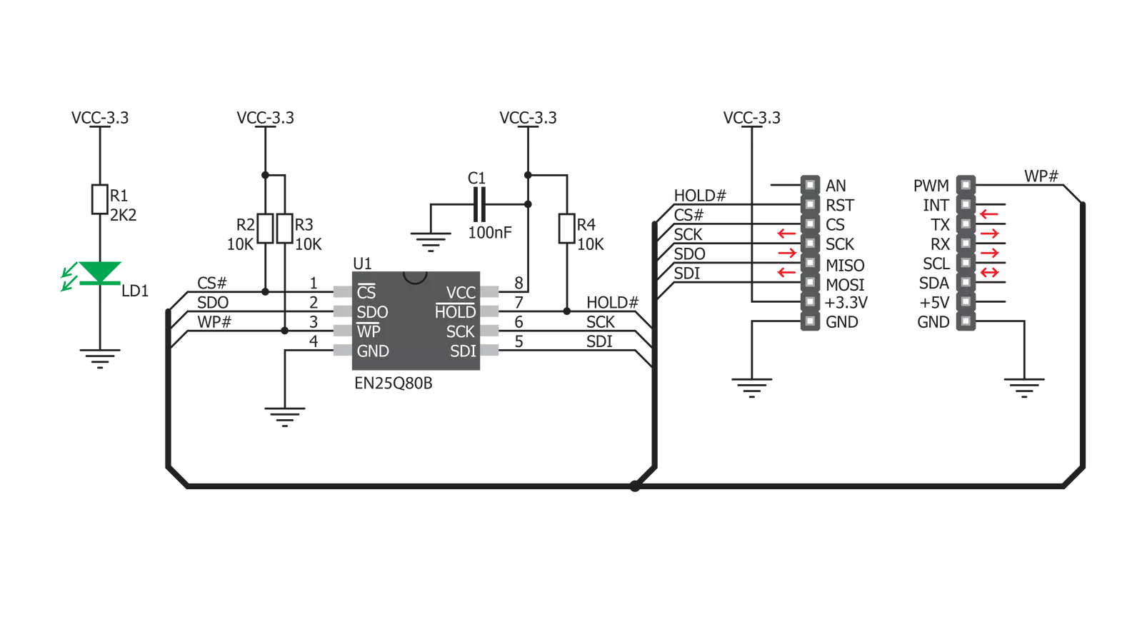
Flash Click is based on the EN25Q80B, a serial flash memory from EON Silicon Solutions. The EN25Q80B features Serial Flash Discoverable Parameters (SFDP) mode, used to retrieve advanced information from the device, such as the operating characteristics, structure and vendor-specified information, memory size, operating voltage, timing information, and more. Page Program instruction allows up to 256 bytes to be written during one write cycle, although it is possible to write less than that. By automatically incrementing the addresses, it is possible to read the entire memory by a single command. The
EN25Q80B allows the erasure of one sector at a time, half a block at a time, block at a time, and the entire memory. The addition of 512 bytes of one-time programmable (OTP) memory can be useful for building secure storage devices and similar secure storage applications. Flash Click uses a standard 4-Wire SPI serial interface to communicate with the host MCU, supporting Dual SPI and Quad SPI modes, which utilize these two additional modes, allowing faster data transfer speeds several times. There are additional WP for the write protect function and HLD pins. If using Quad SPI, the SDI and SDO become DQ0 and
DQ1, while WP and HLD become DQ2 and DQ3, respectively. Due to a small number of MCUs that support Dual and Quad SPI, MIKROE offers library functions that work only with standard SPI communication, ensuring absolute compatibility with all the supported MCUs. This Click board™ can be operated only with a 3.3V logic voltage level. The board must perform appropriate logic voltage level conversion before using MCUs with different logic levels. Also, it comes equipped with a library containing functions and an example code that can be used as a reference for further development.

Features overview
Development board
Arduino UNO is a versatile microcontroller board built around the ATmega328P chip. It offers extensive connectivity options for various projects, featuring 14 digital input/output pins, six of which are PWM-capable, along with six analog inputs. Its core components include a 16MHz ceramic resonator, a USB connection, a power jack, an
ICSP header, and a reset button, providing everything necessary to power and program the board. The Uno is ready to go, whether connected to a computer via USB or powered by an AC-to-DC adapter or battery. As the first USB Arduino board, it serves as the benchmark for the Arduino platform, with "Uno" symbolizing its status as the
first in a series. This name choice, meaning "one" in Italian, commemorates the launch of Arduino Software (IDE) 1.0. Initially introduced alongside version 1.0 of the Arduino Software (IDE), the Uno has since become the foundational model for subsequent Arduino releases, embodying the platform's evolution.

Microcontroller Overview
MCU Card / MCU

Architecture
AVR
MCU Memory (KB)
32
Silicon Vendor
Microchip
Pin count
28
RAM (Bytes)
2048
You complete me!
Accessories
Click Shield for Arduino UNO has two proprietary mikroBUS™ sockets, allowing all the Click board™ devices to be interfaced with the Arduino UNO board without effort. The Arduino Uno, a microcontroller board based on the ATmega328P, provides an affordable and flexible way for users to try out new concepts and build prototypes with the ATmega328P microcontroller from various combinations of performance, power consumption, and features. The Arduino Uno has 14 digital input/output pins (of which six can be used as PWM outputs), six analog inputs, a 16 MHz ceramic resonator (CSTCE16M0V53-R0), a USB connection, a power jack, an ICSP header, and reset button. Most of the ATmega328P microcontroller pins are brought to the IO pins on the left and right edge of the board, which are then connected to two existing mikroBUS™ sockets. This Click Shield also has several switches that perform functions such as selecting the logic levels of analog signals on mikroBUS™ sockets and selecting logic voltage levels of the mikroBUS™ sockets themselves. Besides, the user is offered the possibility of using any Click board™ with the help of existing bidirectional level-shifting voltage translators, regardless of whether the Click board™ operates at a 3.3V or 5V logic voltage level. Once you connect the Arduino UNO board with our Click Shield for Arduino UNO, you can access hundreds of Click boards™, working with 3.3V or 5V logic voltage levels.

Used MCU Pins
mikroBUS™ mapper
Take a closer look
Click board™ Schematic
Step by step
Project assembly

Start by selecting your development board and Click board™. Begin with the Arduino UNO Rev3 as your development board.


Software Support
Library Description
This library contains API for Flash Click driver.
Key functions:
flash_write_page- Page Write functionflash_read_page- Page Read functionflash_erase_sector- Sector Erase function
Open Source
Code example
The complete application code and a ready-to-use project are available through the NECTO Studio Package Manager for direct installation in the NECTO Studio. The application code can also be found on the MIKROE GitHub account.
/*!
 * \file main.c
 * \brief Flash Click example
 *
 * # Description
 * This example demonstrates the use (control) of the FLASH memory.
 *
 * The demo application is composed of two sections :
 *
 * ## Application Init
 * Initializes all necessary peripherals and pins used by Flash Click and also
 * initializes uart logger to show results.
 *
 * ## Application Task
 * Executes memory data writing, reading from the memory to verify data writing
 * operation and sector erasing to clear memory.
 *
 * ## Additional Functions
 * - Enter Data / Allows user to enter a desired data.
 * - Process Wait / Makes a delay to wait while some process be done.
 *
 * \author Nemanja Medakovic
 *
 */
// ------------------------------------------------------------------- INCLUDES

#include <string.h>
#include "board.h"
#include "log.h"
#include "flash.h"

// ------------------------------------------------------------------ VARIABLES

static flash_t flash;
static log_t logger;
static uint8_t data_buf[ 30 ];
static uint8_t n_data;

// ------------------------------------------------------- ADDITIONAL FUNCTIONS

void enter_data( unsigned char *buffer )
{
    uint8_t data_size;

    data_size = sizeof( data_buf );

    memset( data_buf, 0, data_size );
    n_data = 0;
    data_size--;

    while ( ( *buffer != 0 ) && ( data_size > 0 ) )
    {
        data_buf[ n_data ] = *buffer;
        buffer++;
        n_data++;
        data_size--;
    }
}

void process_wait( void )
{
    uint8_t cnt;

    for ( cnt = 0; cnt < 9; cnt++ )
    {
        Delay_ms ( 400 );
        log_printf( &logger, "****" );
    }

    log_printf( &logger, "\r\n" );
    Delay_ms ( 400 );
}

// ------------------------------------------------------ APPLICATION FUNCTIONS

void application_init( void )
{
    flash_cfg_t flash_cfg;
    log_cfg_t log_cfg;

    /**
     * Logger initialization.
     * Default baud rate: 115200
     * Default log level: LOG_LEVEL_DEBUG
     * @note If USB_UART_RX and USB_UART_TX
     * are defined as HAL_PIN_NC, you will
     * need to define them manually for log to work.
     * See @b LOG_MAP_USB_UART macro definition for detailed explanation.
     */
    LOG_MAP_USB_UART( log_cfg );
    log_init( &logger, &log_cfg );
    log_info( &logger, "---- Application Init ----" );

    //  Click initialization.
    flash_cfg_setup( &flash_cfg );
    FLASH_MAP_MIKROBUS( flash_cfg, MIKROBUS_1 );
    flash_init( &flash, &flash_cfg );

    //  Click reset and default configuration.
    flash_reset( &flash );
    flash_default_cfg( &flash );

    log_printf( &logger, "***  Flash Initialization Done.  ***\r\n" );
    log_printf( &logger, "************************************\r\n" );
}

void application_task( void )
{
    enter_data( "Mikroelektronika (MikroE)" );

    log_printf( &logger, "> Data content to be written: %s\r\n", data_buf );
    log_printf( &logger, "> Data writing to memory...\r\n" );
    flash_write_page( &flash, FLASH_MEM_ADDR_FIRST_PAGE_START, data_buf, n_data );
    log_printf( &logger, "> Done.\r\n" );

    memset( data_buf, 0, sizeof( data_buf ) );
    process_wait( );

    log_printf( &logger, "> Data reading from memory...\r\n" );
    flash_read_page( &flash, FLASH_MEM_ADDR_FIRST_PAGE_START, data_buf, n_data );
    log_printf( &logger, "> Done.\r\n> Read data content: %s\r\n", data_buf );

    process_wait( );

    log_printf( &logger, "> Sector erasing...\r\n" );
    flash_erase_sector( &flash, FLASH_MEM_ADDR_FIRST_SECTOR_START );
    log_printf( &logger, "> Done.\r\n" );

    process_wait( );
}

int main ( void )
{
    /* Do not remove this line or clock might not be set correctly. */
    #ifdef PREINIT_SUPPORTED
    preinit();
    #endif

    application_init( );

    for ( ; ; )
    {
        application_task( );
    }

    return 0;
}


// ------------------------------------------------------------------------ END
Additional Support
Resources
Category:FLASH


