Step into the world of digital data with MCP3551 and STM32F030R8
Where analog meets digital

Published Feb 26, 2024
Click board™
ADC 2 Click
Dev Board
Nucleo-64 with STM32F030R8 MCU
Compiler
NECTO Studio
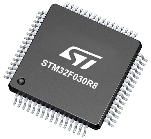
MCU
STM32F030R8
Don't let accuracy be a limiting factor in your data acquisition solutions – try our ADC today!
A
A
Hardware Overview
How does it work?
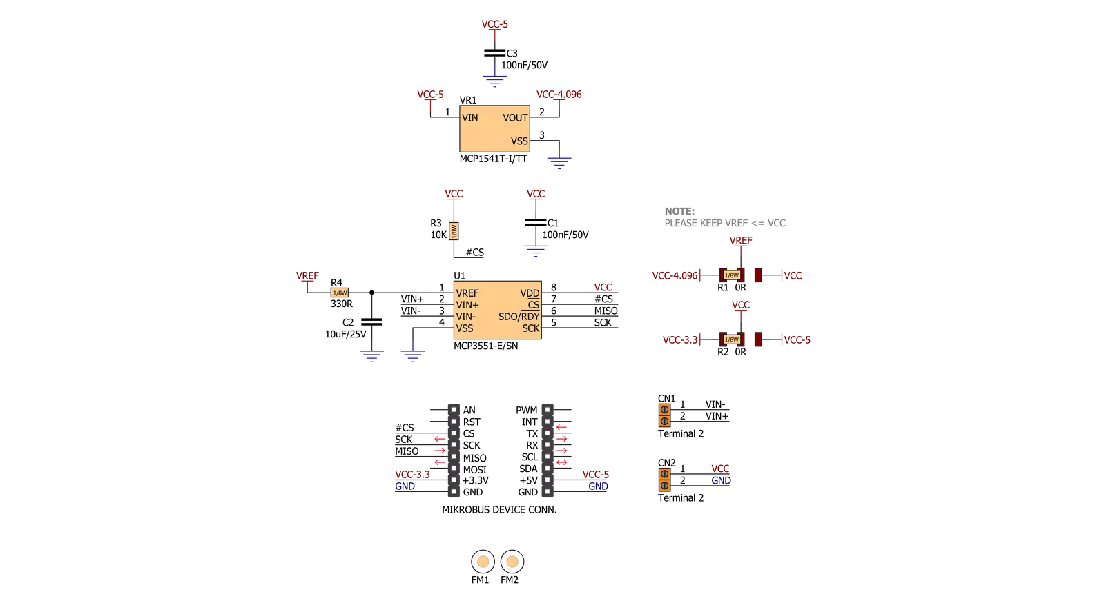
ADC 2 Click is based on the MCP3551, a 22-bit precise single-channel ΔΣ analog-to-digital converter from Microchip. The MCP3551 includes fully differential analog input on a VIN terminal, a third-order delta-sigma modulator, a fourth-order modified SINC decimation filter (allows superior averaging performance), an on-chip, low-noise internal oscillator, a power supply monitoring circuit, and an SPI digital interface. It can be easily used to measure low-frequency, low-level signals such as those found in pressure transducers, temperature, strain gauges, industrial control, or process control applications. This Click board™ communicates with MCU through a 3-Wire SPI interface (read-only) with a maximum frequency of 5MHz. The interface offers two conversion modes: A single Conversion mode for multiplexed
applications and a Continuous Conversion mode for multiple conversions in series, where every conversion is independent of each other (all internal registers are flushed between conversions). When the MCP3551 is not converting, it automatically goes into Shutdown mode, characterized by low power consumption. The MCP3551 provides single-cycle conversions with no digital filter settling time. Every conversion includes an internal offset and gain auto-calibration to reduce device error, which is transparent to the user and done in real-time during the conversion, allowing multiplexed applications. Like any ADC, the MCP3551 uses a reference voltage as the differential voltage range. The reference voltage level selection is performed by positioning the SMD jumper labeled as VREF
SEL to an appropriate position choosing between 3.3V or 5V provided by the mikroBUS™ power rails or 4.096V provided by MCP1541. These voltages may be used as the reference input that results in accuracy and stability. Besides, the ADC 2 Click supports an external power supply for the MCP3551, which can be connected to the input terminal labeled as VCC OUT and should be within the range of 2.7V to 5.5V. This Click board™ can operate with either 3.3V or 5V logic voltage levels selected via the PWR SEL jumper. This way, both 3.3V and 5V capable MCUs can use the communication lines properly. However, the Click board™ comes equipped with a library containing easy-to-use functions and an example code that can be used, as a reference, for further development.

Features overview
Development board
Nucleo-64 with STM32F030R8 MCU offers a cost-effective and adaptable platform for developers to explore new ideas and prototype their designs. This board harnesses the versatility of the STM32 microcontroller, enabling users to select the optimal balance of performance and power consumption for their projects. It accommodates the STM32 microcontroller in the LQFP64 package and includes essential components such as a user LED, which doubles as an ARDUINO® signal, alongside user and reset push-buttons, and a 32.768kHz crystal oscillator for precise timing operations. Designed with expansion and flexibility in mind, the Nucleo-64 board features an ARDUINO® Uno V3 expansion connector and ST morpho extension pin
headers, granting complete access to the STM32's I/Os for comprehensive project integration. Power supply options are adaptable, supporting ST-LINK USB VBUS or external power sources, ensuring adaptability in various development environments. The board also has an on-board ST-LINK debugger/programmer with USB re-enumeration capability, simplifying the programming and debugging process. Moreover, the board is designed to simplify advanced development with its external SMPS for efficient Vcore logic supply, support for USB Device full speed or USB SNK/UFP full speed, and built-in cryptographic features, enhancing both the power efficiency and security of projects. Additional connectivity is
provided through dedicated connectors for external SMPS experimentation, a USB connector for the ST-LINK, and a MIPI® debug connector, expanding the possibilities for hardware interfacing and experimentation. Developers will find extensive support through comprehensive free software libraries and examples, courtesy of the STM32Cube MCU Package. This, combined with compatibility with a wide array of Integrated Development Environments (IDEs), including IAR Embedded Workbench®, MDK-ARM, and STM32CubeIDE, ensures a smooth and efficient development experience, allowing users to fully leverage the capabilities of the Nucleo-64 board in their projects.

Microcontroller Overview
MCU Card / MCU
Architecture
ARM Cortex-M0
MCU Memory (KB)
64
Silicon Vendor
STMicroelectronics
Pin count
64
RAM (Bytes)
8192
You complete me!
Accessories
Click Shield for Nucleo-64 comes equipped with two proprietary mikroBUS™ sockets, allowing all the Click board™ devices to be interfaced with the STM32 Nucleo-64 board with no effort. This way, Mikroe allows its users to add any functionality from our ever-growing range of Click boards™, such as WiFi, GSM, GPS, Bluetooth, ZigBee, environmental sensors, LEDs, speech recognition, motor control, movement sensors, and many more. More than 1537 Click boards™, which can be stacked and integrated, are at your disposal. The STM32 Nucleo-64 boards are based on the microcontrollers in 64-pin packages, a 32-bit MCU with an ARM Cortex M4 processor operating at 84MHz, 512Kb Flash, and 96KB SRAM, divided into two regions where the top section represents the ST-Link/V2 debugger and programmer while the bottom section of the board is an actual development board. These boards are controlled and powered conveniently through a USB connection to program and efficiently debug the Nucleo-64 board out of the box, with an additional USB cable connected to the USB mini port on the board. Most of the STM32 microcontroller pins are brought to the IO pins on the left and right edge of the board, which are then connected to two existing mikroBUS™ sockets. This Click Shield also has several switches that perform functions such as selecting the logic levels of analog signals on mikroBUS™ sockets and selecting logic voltage levels of the mikroBUS™ sockets themselves. Besides, the user is offered the possibility of using any Click board™ with the help of existing bidirectional level-shifting voltage translators, regardless of whether the Click board™ operates at a 3.3V or 5V logic voltage level. Once you connect the STM32 Nucleo-64 board with our Click Shield for Nucleo-64, you can access hundreds of Click boards™, working with 3.3V or 5V logic voltage levels.

Used MCU Pins
mikroBUS™ mapper
Take a closer look
Schematic
Step by step
Project assembly
Start by selecting your development board and Click board™. Begin with the Nucleo-64 with STM32F030R8 MCU as your development board.


Track your results in real time
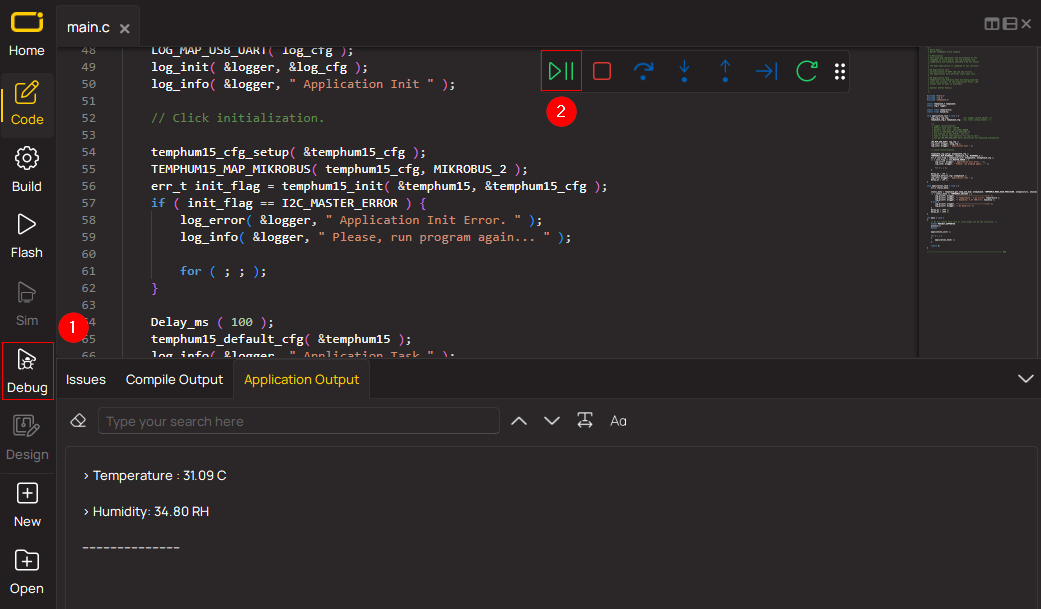
Application Output via Debug Mode
1. Once the code example is loaded, pressing the "DEBUG" button initiates the build process, programs it on the created setup, and enters Debug mode.
2. After the programming is completed, a header with buttons for various actions within the IDE becomes visible. Clicking the green "PLAY" button starts reading the results achieved with the Click board™. The achieved results are displayed in the Application Output tab.
Software Support
Library Description
This library contains API for ADC 2 Click driver.
Key functions:
adc2_adc_Value_Read- Function is used to read specific data from ADC convertor.adc2_check_Over_Low- Function is used to check overflow low state.adc2_check_Over_High- Function is used to check overflow high state.
Open Source
Code example
This example can be found in NECTO Studio. Feel free to download the code, or you can copy the code below.
/*!
 * \file
 * \brief Adc2 Click example
 *
 * # Description
 * This application enables usage of the 22bit ADC.
 *
 * The demo application is composed of two sections :
 *
 * ## Application Init
 * Initalizes SPI driver and makes an initial log.
 *
 * ## Application Task
 * This is an example that shows the capabilities of the ADC 2 click
 *
 *
 * \author MikroE Team
 *
 */
// ------------------------------------------------------------------- INCLUDES

#include "board.h"
#include "log.h"
#include "adc2.h"

// ------------------------------------------------------------------ VARIABLES

static adc2_t adc2;
static log_t logger;

// ------------------------------------------------------ APPLICATION FUNCTIONS

void application_init ( void )
{
    log_cfg_t log_cfg;
    adc2_cfg_t cfg;

    /**
     * Logger initialization.
     * Default baud rate: 115200
     * Default log level: LOG_LEVEL_DEBUG
     * @note If USB_UART_RX and USB_UART_TX
     * are defined as HAL_PIN_NC, you will
     * need to define them manually for log to work.
     * See @b LOG_MAP_USB_UART macro definition for detailed explanation.
     */
    LOG_MAP_USB_UART( log_cfg );
    log_init( &logger, &log_cfg );
    log_info( &logger, "---- Application Init ----" );

    //  Click initialization.

    adc2_cfg_setup( &cfg );
    ADC2_MAP_MIKROBUS( cfg, MIKROBUS_1 );
    adc2_init( &adc2, &cfg );

    Delay_ms( 100 );

    adc2_set_vref( &adc2, ADC2_VCC_3v3 );

    log_printf( &logger, "------------------\r\n" );
    log_printf( &logger, "    ADC 2 Click   \r\n" );
    log_printf( &logger, "------------------\r\n" );
}

void application_task ( void )
{
    float adc_val;

    //  Task implementation.

    adc_val = adc2_read_adc_data( &adc2 );

    log_printf( &logger, "Value : %.2f mV\r\n", adc_val );

    if ( adc2.ovf_h )
        log_printf( &logger, "HIGH OVERFLOW DETECTED\r\n" );
    else if ( adc2.ovf_l )
        log_printf( &logger, "LOW OVERFLOW DETECTED\r\n" );

    log_printf( &logger, "------------------\r\n" );
    Delay_ms( 500 );
}

void main ( void )
{
    application_init( );

    for ( ; ; )
    {
        application_task( );
    }
}


// ------------------------------------------------------------------------ END


