Experience smart power management like never before with MIC2230 and STM32F091RC
Dual synchronous DC/DC regulator

Published Feb 26, 2024
Click board™
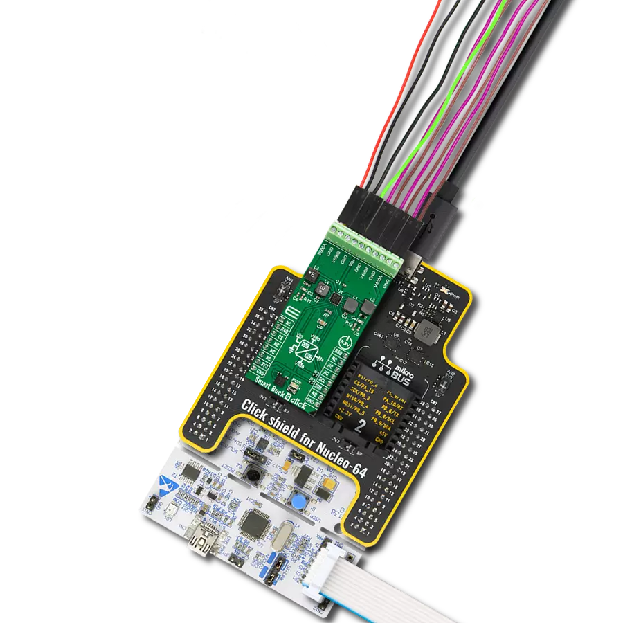
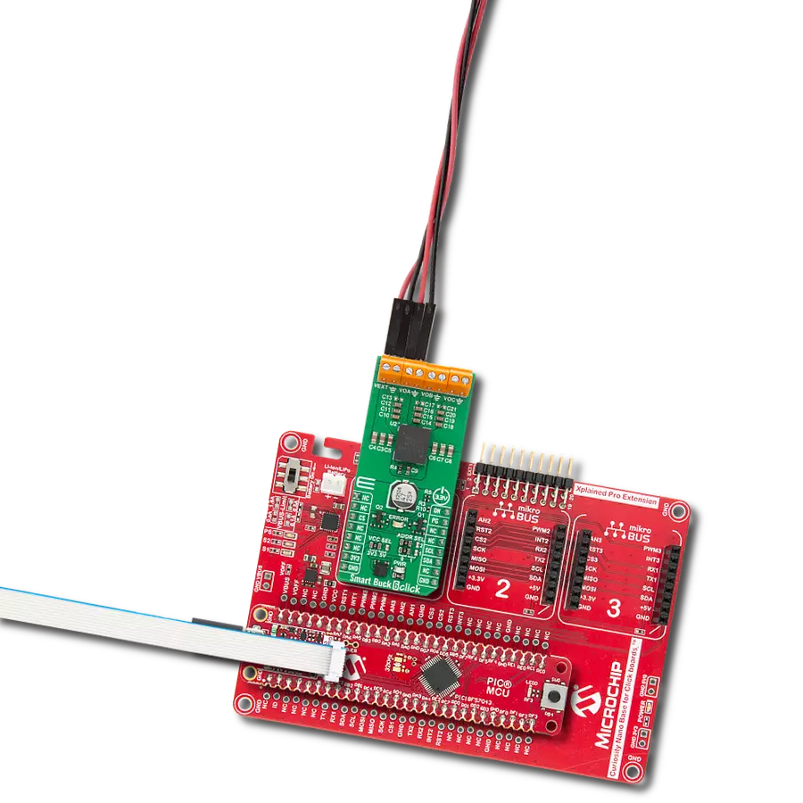
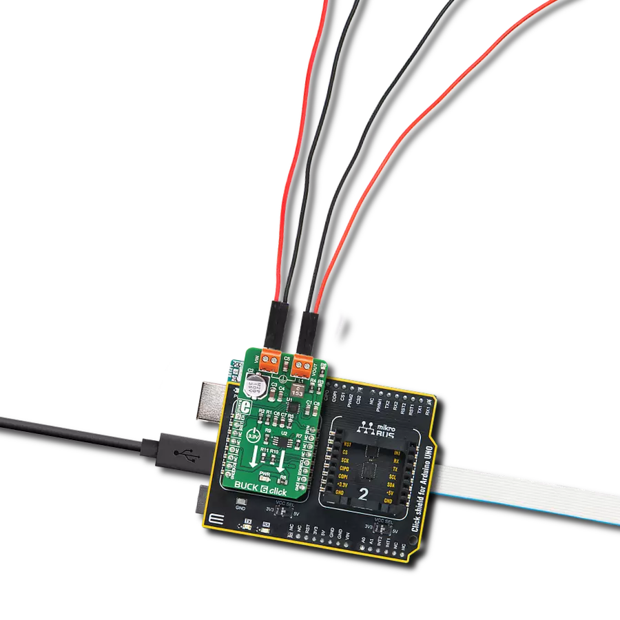
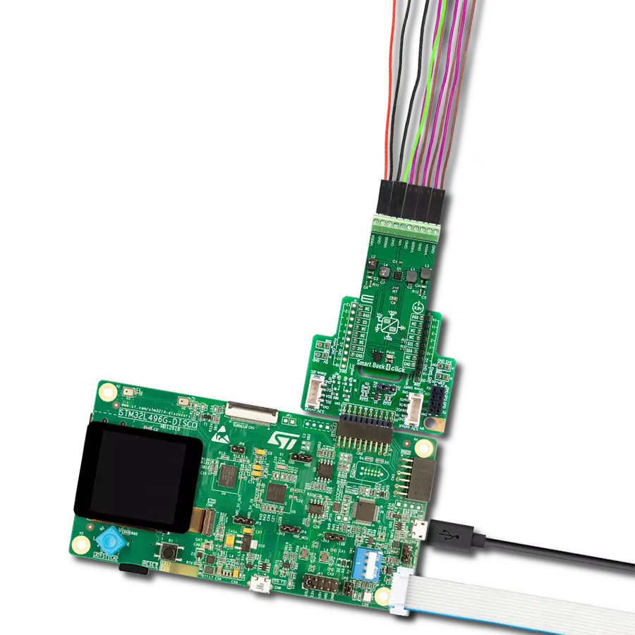
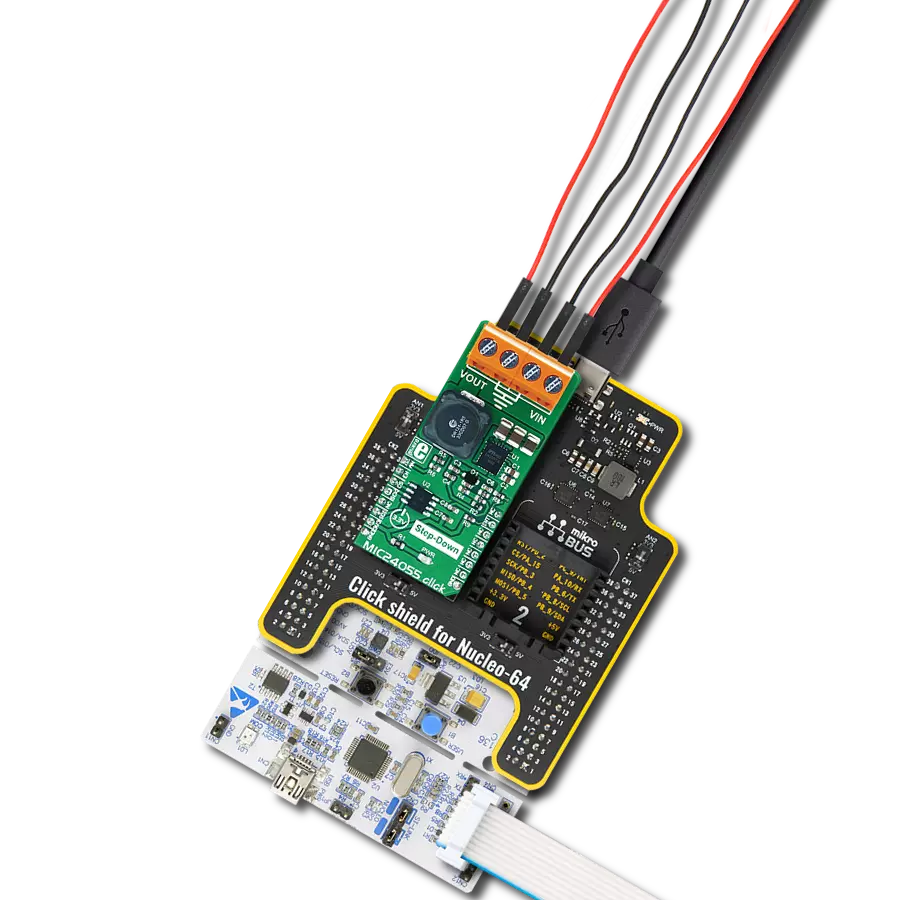
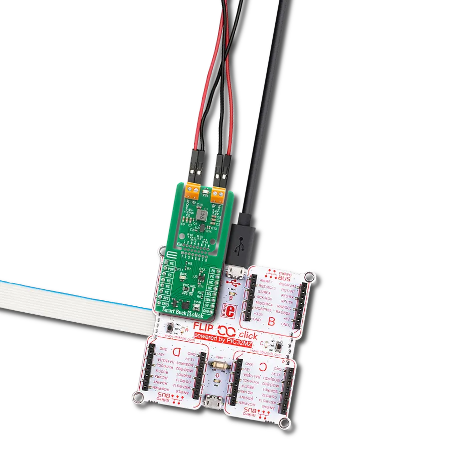
Smart Buck click
Dev. board
Nucleo-64 with STM32F091RC MCU
Compiler
NECTO Studio
MCU
STM32F091RC
Solution ideally suited for portable and embedded systems that demand high power conversion efficiencies and fast transient performance
A
A
Hardware Overview
How does it work?
Smart Buck Click is based on the MIC2230, a dual synchronous step-down DC/DC regulator, by Microchip. This dual buck converter and voltage regulator offers two independent outputs with feedback loops, allowing both outputs to be set to a specific voltage independently. The dual buck converter works in synchronous PWM mode whenever the load drains over 100mA. The operating mode of the converter is switched to the so-called Trickle mode when the connected load drains less than 100mA. Although highly efficient for light loads, this mode has its downsides, such as the slightly increased ripple and increased voltage regulation tolerance. This is sufficient for most cases (when the supplied device enters the standby mode, when the system is suspended, and similar). Still, for some critical low current applications, the MIC2230 can always operate in synchronous PWM mode at 2.5MHz, with the output voltage ripple as low as 7mV. To set the PWM mode regardless of the connected load, pulling the FPWM pin of the MIC2230 to a LOW logic level is sufficient. The FPWM pin is routed to the PWM pin of the mikroBUS™. Two FB pins of the MIC2230 are used to determine the output voltage at each output. A digitally controlled dual potentiometer IC is on the Click board™, labeled as the MCP4661. This IC is a dual 8-bit digital potentiometer with non-volatile memory and the WiperLock function from Microchip. The WiperLock function allows the permanent storage of the wiper position in the internal EEPROM of the MCP4661 IC. The internal digital potentiometers are connected as the rheostats, acting as the second variable resistor of the feedback voltage dividers. This allows setting the output voltage by programming the digital potentiometer values via the I2C interface. The I2C
slave address of the MCP4661 IC can be set by the SMD jumpers, labeled as A0 to A2, grouped under the MCP4661 label. Smart Buck Click uses the PAC1934, a four-channel DC power and energy monitor with the accumulator, for power monitoring purposes, from Microchip. Due to its high degree of integration and an integrated real-time offset and gain compensation circuitry, this device requires only a few sensing resistors to monitor the voltage and sense the current consumption. This IC also contains a high-performance digital section, accessible via the I2C interface, which is used to integrate the measurement results and provide on-chip power calculations, reducing the processing load of the MCU. Single Shot and Continous modes are at disposal, allowing fine-tuning of its functionality. It has four channels, of which two are used to monitor current and voltage on the two output terminals. One of the channels is used to monitor power consumption on the input supply terminal, and finally, one channel monitors the +5V rail of the mikroBUS™. This allows the power efficiency of the converter to be easily calculated, as well as the power consumption of the Click board™ as a whole. The sensing elements connected to the PAC1934 are low-value resistors, ranging from 0.05Ω to 0.11Ω. The channel inputs are differential pairs implemented as the Kelvin connection to sensing resistors. Kelvin connection allows precise measurements since the voltage drop along the sensor traces, due to their resistance, is eliminated. The I2C address of the PAC1934 monitoring IC can also be changed by the onboard SMD jumper, labeled PAC1934 ADDR SEL. The sampling rate can also be changed by switching the SLOW SAMP jumper to either 0 or 1. Switching it to 1 will enable the slow sampling feature of the PAC1934,
enforcing the sample rate of 8sps, regardless of the CTRL register content. The default sampling rate with the default jumper position (SLOW SAMP at 0) is 1024sps. An EEPROM module is included onboard as an extra feature of the Smart Buck click. The 24C02C, an I2C serial EEPROM from Microchip with a density of 2kbit, is used on the Click board™ to provide storage for any data. It has 2kbit of memory, organized in 256 x 8bit words, which translates to 256 bytes of non-volatile memory, which can be used to store working parameters or other application-specific data. The outstanding quality of the module allows up to one million write/erase cycles and data retention of more than 200 years. All its inputs are protected from noise with the Schmitt triggers, and the module supports fast-speed I2C mode, up to 400kHz. The I2C address of this device is also configurable by a set of SMD jumpers labeled A0 to A2, grouped under the 24C02 label. The input/output facilities include two terminals labeled CH1 and CH2, which output the step-down voltage in the range of 0.8V up to 5.5V, as previously mentioned. A notice should be taken that an input voltage of up to 5.5V should be connected at the input terminal labeled as the VIN to get a voltage at the output. Also, it should be noted that the output voltage should always be programmed to a value lower than the input voltage. An external power supply at the VIN terminal will be indicated by a red LED labeled EXT PWR. The I2C protocol is used for all the sections of Smart Buck click. The required pull-up resistors are included onboard. The Click board™ allows interfacing with 3.3V MCUs, only.

Features overview
Development board
Nucleo-64 with STM32F091RC MCU offers a cost-effective and adaptable platform for developers to explore new ideas and prototype their designs. This board harnesses the versatility of the STM32 microcontroller, enabling users to select the optimal balance of performance and power consumption for their projects. It accommodates the STM32 microcontroller in the LQFP64 package and includes essential components such as a user LED, which doubles as an ARDUINO® signal, alongside user and reset push-buttons, and a 32.768kHz crystal oscillator for precise timing operations. Designed with expansion and flexibility in mind, the Nucleo-64 board features an ARDUINO® Uno V3 expansion connector and ST morpho extension pin
headers, granting complete access to the STM32's I/Os for comprehensive project integration. Power supply options are adaptable, supporting ST-LINK USB VBUS or external power sources, ensuring adaptability in various development environments. The board also has an on-board ST-LINK debugger/programmer with USB re-enumeration capability, simplifying the programming and debugging process. Moreover, the board is designed to simplify advanced development with its external SMPS for efficient Vcore logic supply, support for USB Device full speed or USB SNK/UFP full speed, and built-in cryptographic features, enhancing both the power efficiency and security of projects. Additional connectivity is
provided through dedicated connectors for external SMPS experimentation, a USB connector for the ST-LINK, and a MIPI® debug connector, expanding the possibilities for hardware interfacing and experimentation. Developers will find extensive support through comprehensive free software libraries and examples, courtesy of the STM32Cube MCU Package. This, combined with compatibility with a wide array of Integrated Development Environments (IDEs), including IAR Embedded Workbench®, MDK-ARM, and STM32CubeIDE, ensures a smooth and efficient development experience, allowing users to fully leverage the capabilities of the Nucleo-64 board in their projects.

Microcontroller Overview
MCU Card / MCU

Architecture
ARM Cortex-M0
MCU Memory (KB)
256
Silicon Vendor
STMicroelectronics
Pin count
64
RAM (Bytes)
32768
You complete me!
Accessories
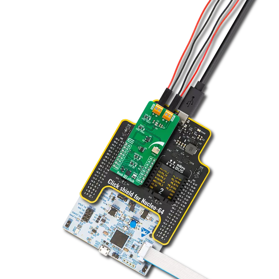
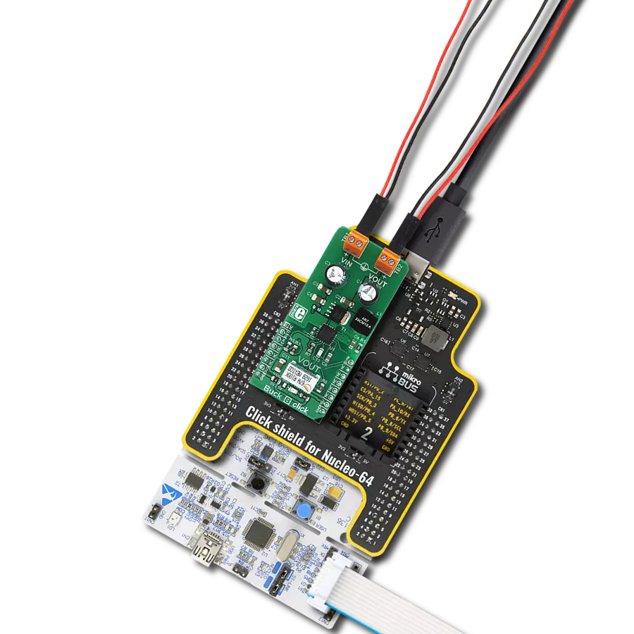
Click Shield for Nucleo-64 comes equipped with two proprietary mikroBUS™ sockets, allowing all the Click board™ devices to be interfaced with the STM32 Nucleo-64 board with no effort. This way, Mikroe allows its users to add any functionality from our ever-growing range of Click boards™, such as WiFi, GSM, GPS, Bluetooth, ZigBee, environmental sensors, LEDs, speech recognition, motor control, movement sensors, and many more. More than 1537 Click boards™, which can be stacked and integrated, are at your disposal. The STM32 Nucleo-64 boards are based on the microcontrollers in 64-pin packages, a 32-bit MCU with an ARM Cortex M4 processor operating at 84MHz, 512Kb Flash, and 96KB SRAM, divided into two regions where the top section represents the ST-Link/V2 debugger and programmer while the bottom section of the board is an actual development board. These boards are controlled and powered conveniently through a USB connection to program and efficiently debug the Nucleo-64 board out of the box, with an additional USB cable connected to the USB mini port on the board. Most of the STM32 microcontroller pins are brought to the IO pins on the left and right edge of the board, which are then connected to two existing mikroBUS™ sockets. This Click Shield also has several switches that perform functions such as selecting the logic levels of analog signals on mikroBUS™ sockets and selecting logic voltage levels of the mikroBUS™ sockets themselves. Besides, the user is offered the possibility of using any Click board™ with the help of existing bidirectional level-shifting voltage translators, regardless of whether the Click board™ operates at a 3.3V or 5V logic voltage level. Once you connect the STM32 Nucleo-64 board with our Click Shield for Nucleo-64, you can access hundreds of Click boards™, working with 3.3V or 5V logic voltage levels.

Used MCU Pins
mikroBUS™ mapper
Take a closer look
Click board™ Schematic

Step by step
Project assembly
Start by selecting your development board and Click board™. Begin with the Nucleo-64 with STM32F091RC MCU as your development board.


Software Support
Library Description
This library contains API for Smart Buck Click driver.
Key functions:
smartbuck_send_cmd_PAC- Function performs the desired command for PAC1934smartbuck_get_data- Function reads and calculates the voltage, current and power data from PAC1934 activated channelssmartbuck_block_read_PAC- Function reads the desired number of bytes from the PAC1934 registers
Open Source
Code example
The complete application code and a ready-to-use project are available through the NECTO Studio Package Manager for direct installation in the NECTO Studio. The application code can also be found on the MIKROE GitHub account.
/*!
* \file
* \brief SMARTBUCK Click example
*
* # Description
* This application reads voltage, current, and power from all available channels.
*
* The demo application is composed of two sections :
*
* ## Application Init
* Initializes I2C interface and logger and peforms the Click default configuration.
*
* ## Application Task
* Sends command for updating data registers with new converted data,
* then waits 500ms and after that reads new data from data registers.
* In this way we can get voltage, current and power data from activated channels.
* Results are being logged on USB UART.
*
* \author MikroE Team
*
*/
// ------------------------------------------------------------------- INCLUDES
#include "board.h"
#include "log.h"
#include "smartbuck.h"
// ------------------------------------------------------------------ VARIABLES
static smartbuck_t smartbuck;
static log_t logger;
float voltage_res[ 4 ];
float current_res[ 4 ];
float power_res[ 4 ];
uint8_t check_byte;
uint8_t cnt;
uint8_t idx;
char text[ 50 ];
// ------------------------------------------------------- ADDITIONAL FUNCTIONS
//Checks which channel is activated (from CH1 to CH4) and logs text on uart
void channel_log()
{
switch ( check_byte )
{
case 0x80 :
{
log_printf( &logger, "\r\nCH1:\t" );
break;
}
case 0x40 :
{
log_printf( &logger, "\r\nCH2:\t" );
break;
}
case 0x20 :
{
log_printf( &logger, "\r\nCH3:\t" );
break;
}
case 0x10 :
{
log_printf( &logger, "\r\nCH4:\t" );
break;
}
default :
{
break;
}
}
}
// ------------------------------------------------------ APPLICATION FUNCTIONS
void application_init ( void )
{
log_cfg_t log_cfg;
smartbuck_cfg_t cfg;
/**
* Logger initialization.
* Default baud rate: 115200
* Default log level: LOG_LEVEL_DEBUG
* @note If USB_UART_RX and USB_UART_TX
* are defined as HAL_PIN_NC, you will
* need to define them manually for log to work.
* See @b LOG_MAP_USB_UART macro definition for detailed explanation.
*/
LOG_MAP_USB_UART( log_cfg );
log_init( &logger, &log_cfg );
log_info( &logger, "---- Application Init ----" );
// Click initialization.
smartbuck_cfg_setup( &cfg );
SMARTBUCK_MAP_MIKROBUS( cfg, MIKROBUS_1 );
smartbuck_init( &smartbuck, &cfg );
smartbuck_default_cfg( &smartbuck );
}
void application_task ( void )
{
smartbuck_send_cmd_pac( &smartbuck, SMARTBUCK_REFRESH_V_CMND );
Delay_ms ( 500 );
smartbuck_get_data( &smartbuck, &voltage_res[ 0 ], ¤t_res[ 0 ], &power_res[ 0 ] );
check_byte = 0x80;
idx = 0;
for ( cnt = 0; cnt < 4; cnt++ )
{
if ( ( smartbuck.enabled_chann & check_byte ) == 0 )
{
channel_log();
log_printf( &logger, "U: %.2f V ", voltage_res[ idx ] );
log_printf( &logger, "I: %.2f mA ", current_res[ idx ] );
log_printf( &logger, "P: %.2f mW ", power_res[ idx ] );
idx++;
}
check_byte >>= 1;
}
log_printf( &logger, "\n");
}
int main ( void )
{
/* Do not remove this line or clock might not be set correctly. */
#ifdef PREINIT_SUPPORTED
preinit();
#endif
application_init( );
for ( ; ; )
{
application_task( );
}
return 0;
}
// ------------------------------------------------------------------------ END
Additional Support
Resources
Category:Buck