Experience next-gen power management with MAX17504 and STM32F031K6
Buck the voltage, embrace the efficiency

Published Oct 01, 2024
Click board™
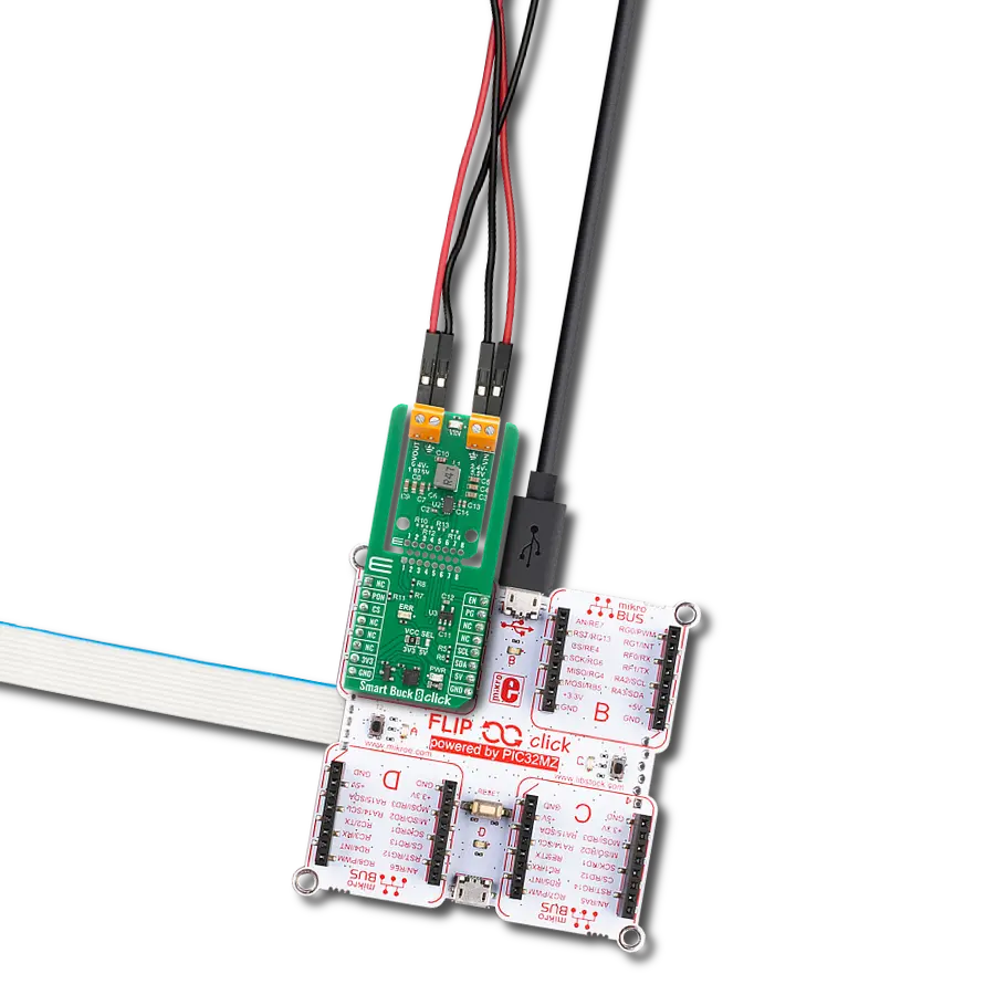
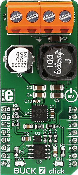
BUCK 7 Click
Dev. board
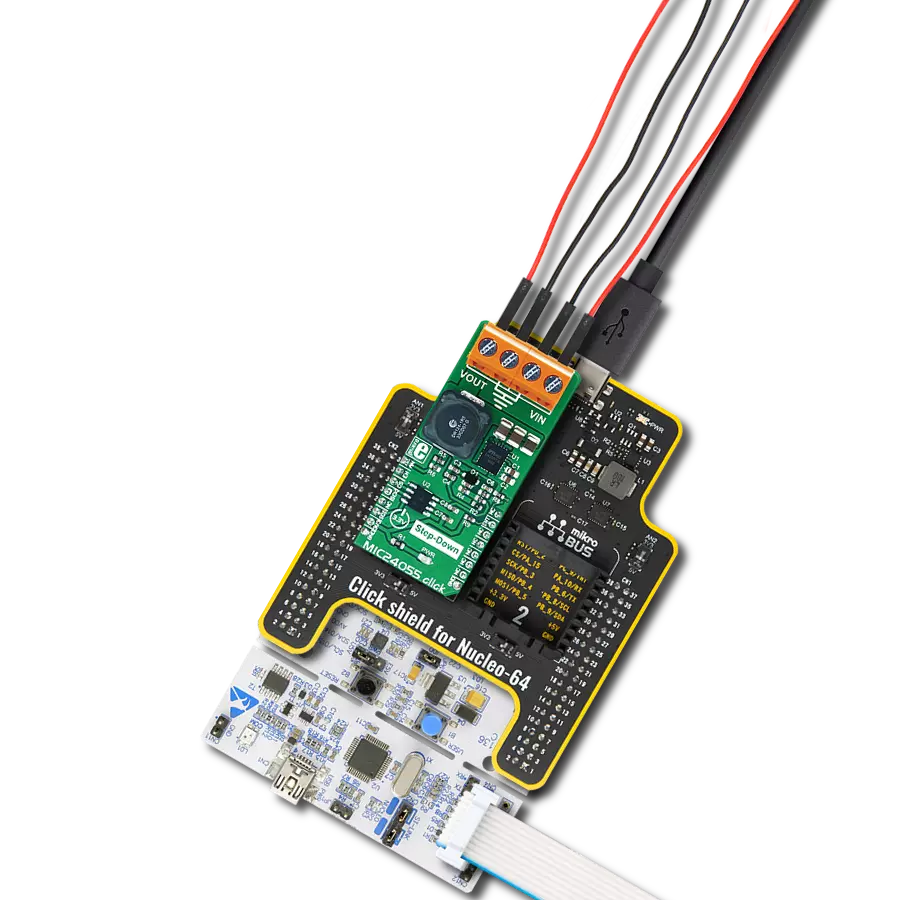
Nucleo 32 with STM32F031K6 MCU
Compiler
NECTO Studio
MCU
STM32F031K6
Don't compromise on voltage stability. Choose this voltage step-down solution, and regulate from 5V up to 35V!
A
A
Hardware Overview
How does it work?
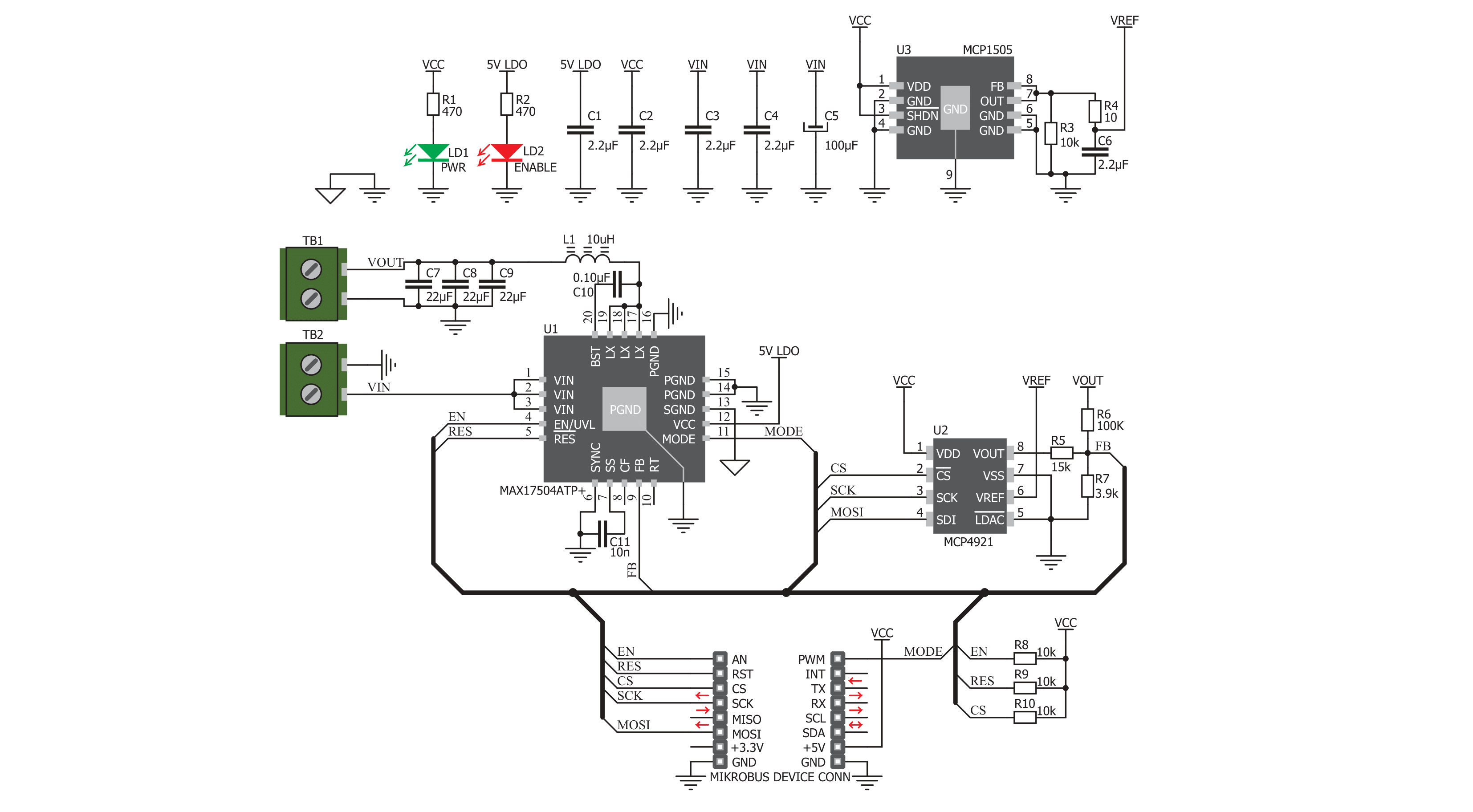
Buck 7 Click is based on the MAX17504, a high-efficiency, synchronous step-down DC-DC converter with internal compensation from Analog Devices. This advanced integrated step-down converter requires a minimum number of external components, thanks to the internal feedback loop compensation. It utilizes a peak-current-mode control architecture, meaning that while the high side MOSFET is open and the current through the inductor ramps up, an overcurrent event will cause the MOSFET to close, preventing this current from becoming dangerously high. If there is a short circuit condition on the output, the device will reattempt to start after a timeout period, and if the condition is still present at the output, it will be turned off for another timeout period. The MCP4921, a 12-bit D/A converter with SPI Interface made by Microchip, is used on the feedback loop to allow adjustment of the output voltage via the SPI interface. This DAC affects the current through the feedback loop forcing the PWM duty cycle of the internal generator, regulating the output voltage to a programmed value that way. As a result, sending a digital value through the SPI interface to the MCP4921 makes it possible to control the output
voltage level in the range from 3.3V to 90% of the input voltage value. While operating normally (PWM mode), the high and the low side MOSFETs are switched synchronously with the signal from the internal PWM generator, causing the current through the inductor to ramp up and down, regulating the output voltage that way. The PWM signal's lower pulse width (duty cycle) results in a lower voltage at the output. Besides PWM mode, the device can also operate in the PFM mode (Pulse Frequency Modulation). This mode allows even higher efficiency for light loads, as the low-side MOSFET is completely unused. The high side MOSFET charges the inductor, letting the load drain it. During this period, the IC is in a hibernation state. This mode results in slightly more ripple at the output, with the added benefit of high efficiency for light loads. It is perfectly suited to power devices in the low power consumption mode (Sleep, Standby, and more). The DCM mode is the compromise mode between the PWM and PFM modes. The low-side MOSFET is still unused for light loads, but the PWM pulses are not skipped, and the IC constantly drives the high-side MOSFET. This mode produces ripple at the output, but it is slightly less efficient than
the PFM mode for light loads. The MODE pin selects different modes. This pin is routed to the mikroBUS™ PWM pin (labeled as MOD), allowing the MCU to control the mode. When set to a HIGH level, the IC works in the DCM mode for light loads. When left floating, the PFM mode is selected. When it is set to the LOW logic level, the constant frequency PWM mode is set. The #RES pin of the IC is routed to the mikroBUS™ RST pin. This pin signalizes problems with the output voltage. The pin is driven to a LOW logic level when the output voltage drops under 92% of the nominal value or during the thermal shutdown. It is an open drain output, otherwise pulled to a HIGH logic level (when not asserted). To enable the buck converter IC, a HIGH logic level needs to be present at the EN pin of the IC, routed to the mikroBUS™ AN pin (labeled as EN). This allows the MCU to control the Power ON function of the Click board™ effectively. When the IC is enabled, the LED indicator labeled EN indicates that the IC is activated and the step-down conversion is in progress. The soft-start circuit prevents high inrush currents by ramping up the output voltage from 0V to the nominal value.

Features overview
Development board
Nucleo 32 with STM32F031K6 MCU board provides an affordable and flexible platform for experimenting with STM32 microcontrollers in 32-pin packages. Featuring Arduino™ Nano connectivity, it allows easy expansion with specialized shields, while being mbed-enabled for seamless integration with online resources. The
board includes an on-board ST-LINK/V2-1 debugger/programmer, supporting USB reenumeration with three interfaces: Virtual Com port, mass storage, and debug port. It offers a flexible power supply through either USB VBUS or an external source. Additionally, it includes three LEDs (LD1 for USB communication, LD2 for power,
and LD3 as a user LED) and a reset push button. The STM32 Nucleo-32 board is supported by various Integrated Development Environments (IDEs) such as IAR™, Keil®, and GCC-based IDEs like AC6 SW4STM32, making it a versatile tool for developers.

Microcontroller Overview
MCU Card / MCU

Architecture
ARM Cortex-M0
MCU Memory (KB)
32
Silicon Vendor
STMicroelectronics
Pin count
32
RAM (Bytes)
4096
You complete me!
Accessories
Click Shield for Nucleo-32 is the perfect way to expand your development board's functionalities with STM32 Nucleo-32 pinout. The Click Shield for Nucleo-32 provides two mikroBUS™ sockets to add any functionality from our ever-growing range of Click boards™. We are fully stocked with everything, from sensors and WiFi transceivers to motor control and audio amplifiers. The Click Shield for Nucleo-32 is compatible with the STM32 Nucleo-32 board, providing an affordable and flexible way for users to try out new ideas and quickly create prototypes with any STM32 microcontrollers, choosing from the various combinations of performance, power consumption, and features. The STM32 Nucleo-32 boards do not require any separate probe as they integrate the ST-LINK/V2-1 debugger/programmer and come with the STM32 comprehensive software HAL library and various packaged software examples. This development platform provides users with an effortless and common way to combine the STM32 Nucleo-32 footprint compatible board with their favorite Click boards™ in their upcoming projects.

Used MCU Pins
mikroBUS™ mapper
Take a closer look
Click board™ Schematic
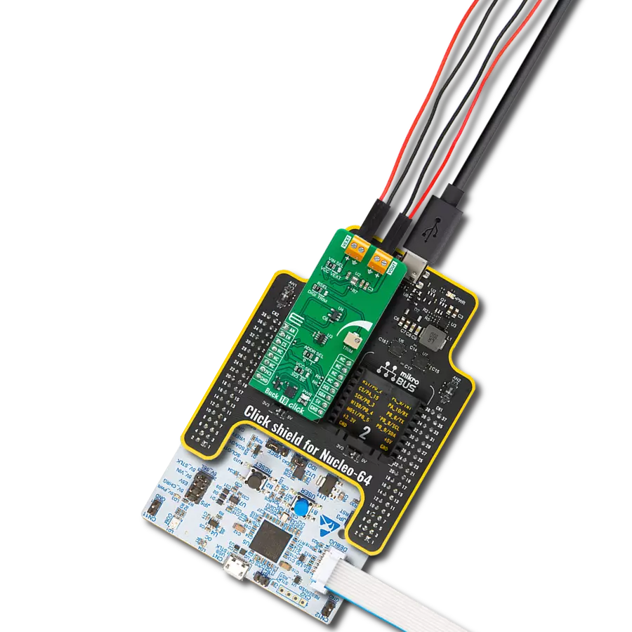
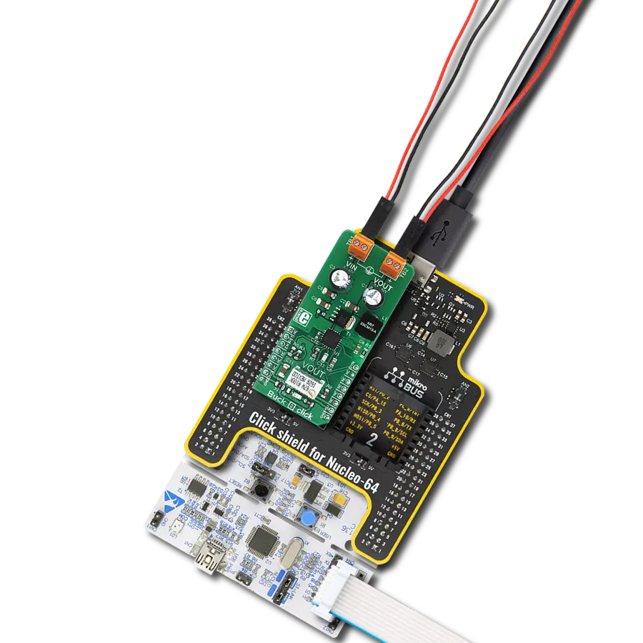
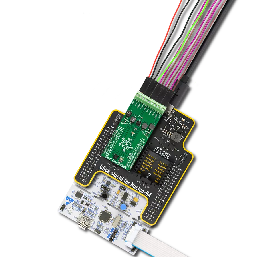
Step by step
Project assembly

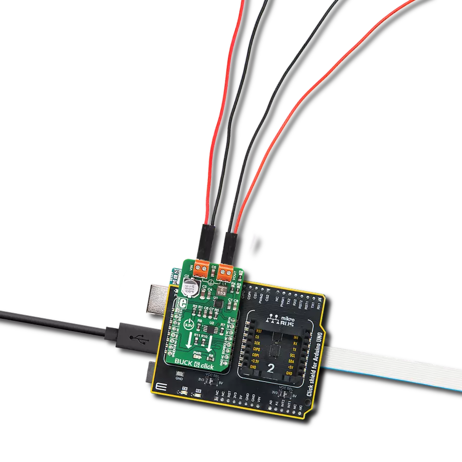
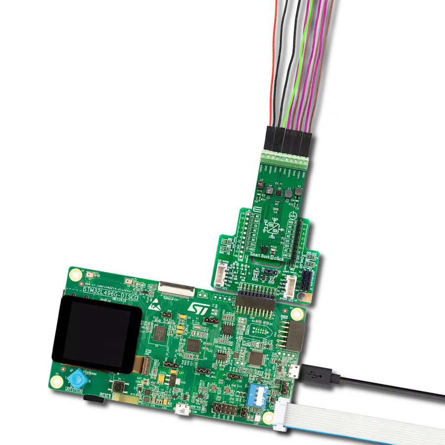
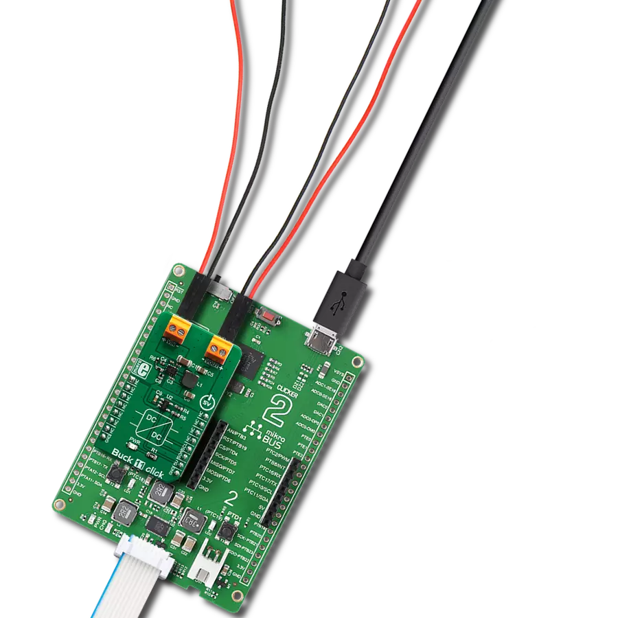
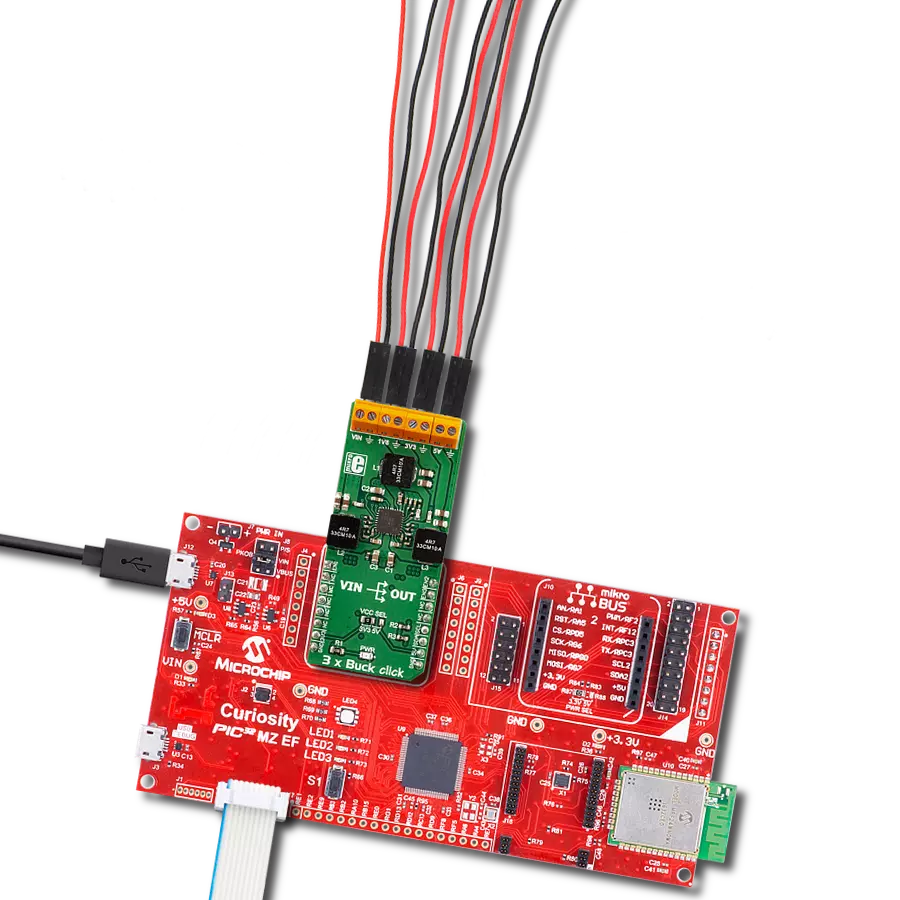
Start by selecting your development board and Click board™. Begin with the Nucleo 32 with STM32F031K6 MCU as your development board.


Software Support
Library Description
This library contains API for Buck 7 Click driver.
Key functions:
buck7_set_output_voltage- Function for settings output voltagebuck7_enable- Function for enable chipbuck7_set_mode- Function for settings chip mode
Open Source
Code example
The complete application code and a ready-to-use project are available through the NECTO Studio Package Manager for direct installation in the NECTO Studio. The application code can also be found on the MIKROE GitHub account.
/*!
 * \file
 * \brief BUCK7 Click example
 *
 * # Description
 * This demo application controls the voltage at the output using the BUCK 7 Click.
 *
 * The demo application is composed of two sections :
 *
 * ## Application Init
 * Initializes Driver init, reset chip, enable chip and set mode
 *
 * ## Application Task
 * Sets output voltage to 5V, 10V, 15V, 20V, 25V every 3 seconds.
 * It is necessary to set the input voltage on 2.7V + maximum output voltage.
 *
 * \author MikroE Team
 *
 */
// ------------------------------------------------------------------- INCLUDES

#include "board.h"
#include "log.h"
#include "buck7.h"

// ------------------------------------------------------------------ VARIABLES

static buck7_t buck7;
static log_t logger;

// ------------------------------------------------------ APPLICATION FUNCTIONS

void application_init ( void )
{
    log_cfg_t log_cfg;
    buck7_cfg_t cfg;

    /**
     * Logger initialization.
     * Default baud rate: 115200
     * Default log level: LOG_LEVEL_DEBUG
     * @note If USB_UART_RX and USB_UART_TX
     * are defined as HAL_PIN_NC, you will
     * need to define them manually for log to work.
     * See @b LOG_MAP_USB_UART macro definition for detailed explanation.
     */
    LOG_MAP_USB_UART( log_cfg );
    log_init( &logger, &log_cfg );
    log_info( &logger, "---- Application Init ----" );

    //  Click initialization.

    buck7_cfg_setup( &cfg );
    BUCK7_MAP_MIKROBUS( cfg, MIKROBUS_1 );
    buck7_init( &buck7, &cfg );

    buck7_enable( &buck7 );
    buck7_set_mode( &buck7, BUCK7_MODE_PWM );
}

void application_task ( )
{
    buck7_set_output_voltage( &buck7, BUCK7_OUT_VOLTAGE_5V );
    Delay_ms ( 1000 );
    Delay_ms ( 1000 );
    Delay_ms ( 1000 );
    buck7_set_output_voltage( &buck7, BUCK7_OUT_VOLTAGE_10V );
    Delay_ms ( 1000 );
    Delay_ms ( 1000 );
    Delay_ms ( 1000 );
    buck7_set_output_voltage( &buck7, BUCK7_OUT_VOLTAGE_15V );
    Delay_ms ( 1000 );
    Delay_ms ( 1000 );
    Delay_ms ( 1000 );
    buck7_set_output_voltage( &buck7, BUCK7_OUT_VOLTAGE_20V );
    Delay_ms ( 1000 );
    Delay_ms ( 1000 );
    Delay_ms ( 1000 );
    buck7_set_output_voltage( &buck7, BUCK7_OUT_VOLTAGE_25V );
    Delay_ms ( 1000 );
    Delay_ms ( 1000 );
    Delay_ms ( 1000 );
    buck7_set_output_voltage( &buck7, BUCK7_OUT_VOLTAGE_20V );
    Delay_ms ( 1000 );
    Delay_ms ( 1000 );
    Delay_ms ( 1000 );
    buck7_set_output_voltage( &buck7, BUCK7_OUT_VOLTAGE_15V );
    Delay_ms ( 1000 );
    Delay_ms ( 1000 );
    Delay_ms ( 1000 );
    buck7_set_output_voltage( &buck7, 0x0BB8 );
    Delay_ms ( 1000 );
    Delay_ms ( 1000 );
    Delay_ms ( 1000 );
}

int main ( void )
{
    /* Do not remove this line or clock might not be set correctly. */
    #ifdef PREINIT_SUPPORTED
    preinit();
    #endif

    application_init( );

    for ( ; ; )
    {
        application_task( );
    }

    return 0;
}


// ------------------------------------------------------------------------ END
Additional Support
Resources
Category:Buck