Easily upgrade and expand storage capacity with SST26VF064B and STM32F031K6
Lightning-fast data waves

Published Oct 01, 2024
Click board™
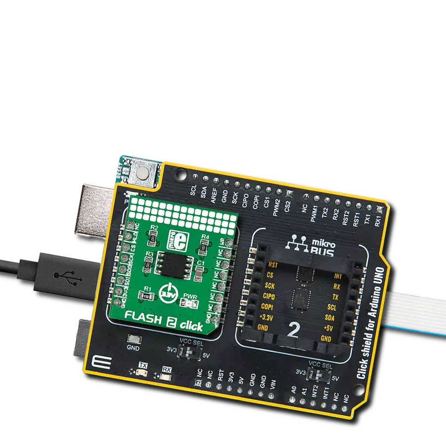
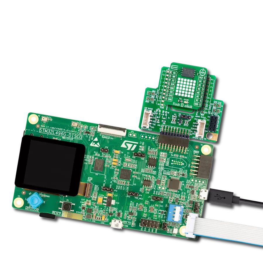
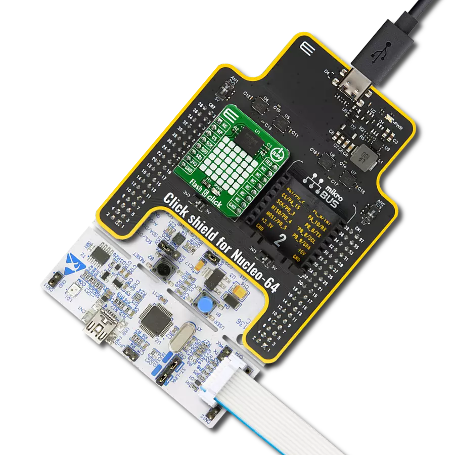
Flash 2 Click
Dev. board
Nucleo 32 with STM32F031K6 MCU
Compiler
NECTO Studio
MCU
STM32F031K6
Harness the capability of flash memory to provide considerably faster read and write speeds than traditional hard drives, thereby elevating the overall performance and responsiveness of the system
A
A
Hardware Overview
How does it work?
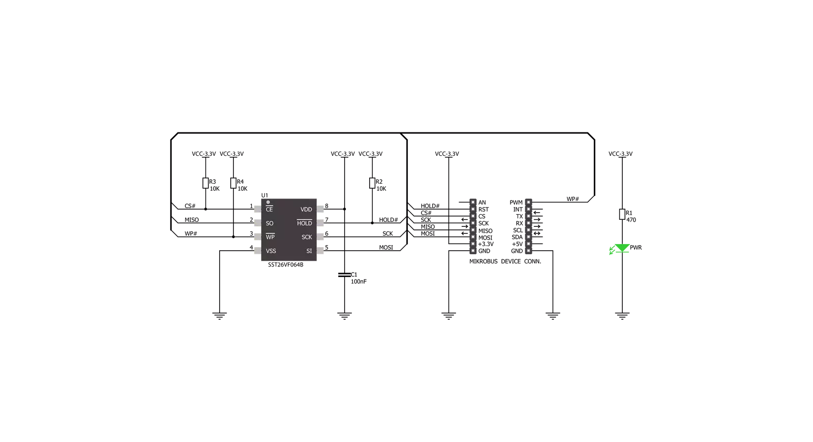
Flash 2 Click is based on the SST26VF064B, a Flash memory chip from Microchip. The Flash memory density is usually expressed in bits, so exactly 67,108,864 bits are organized in units of 8 bits (bytes), which gives 8,388,608 bytes of data memory. This memory module contains 2048 sectors of 4 KB each. Furthermore, the memory is organized into pages. One page holds 256 bytes, and there are 32,768 pages (32,768 pages x 256 bytes = 8,388,608 bytes total). Having insight into how the memory cells are organized is crucial for understanding the Write and Erase operations. The SST26VF064B offers a flexible memory protection scheme that allows each individual block to be write-protected. The addition of 2KB of
one-time programmable (OTP) memory can be useful for building secure storage devices and similar secure storage applications. It can be used to store various security data. Once programmed, this memory can be permanently locked without the possibility to reprogram it ever again. The flash memory IC used on this Click board™ features Serial Flash Discoverable Parameters (SFDP) mode, used to retrieve the advanced information from the device, such as the operating characteristics, structure and vendor specified information, memory size, operating voltage, timing information, and more. Flash 2 Click uses a standard 4-wire SPI serial interface to communicate with the host MCU, supporting
clock frequencies of up to 104MHz. Additional pins routed to the mikroBUS™ include the WP write protect pin, used to put the device into the hardware write protect mode, and the HLD hold pin, used to hold the data transfer. Flash 2 Click also supports Quad SPI mode, in which the WP and HLD pins become SO2 and SO3. This Click board™ can be operated only with a 3.3V logic voltage level. The board must perform appropriate logic voltage level conversion before using MCUs with different logic levels. Also, this Click board™ comes equipped with a library containing easy-to-use functions and an example code that can be used as a reference for further development.

Features overview
Development board
Nucleo 32 with STM32F031K6 MCU board provides an affordable and flexible platform for experimenting with STM32 microcontrollers in 32-pin packages. Featuring Arduino™ Nano connectivity, it allows easy expansion with specialized shields, while being mbed-enabled for seamless integration with online resources. The
board includes an on-board ST-LINK/V2-1 debugger/programmer, supporting USB reenumeration with three interfaces: Virtual Com port, mass storage, and debug port. It offers a flexible power supply through either USB VBUS or an external source. Additionally, it includes three LEDs (LD1 for USB communication, LD2 for power,
and LD3 as a user LED) and a reset push button. The STM32 Nucleo-32 board is supported by various Integrated Development Environments (IDEs) such as IAR™, Keil®, and GCC-based IDEs like AC6 SW4STM32, making it a versatile tool for developers.

Microcontroller Overview
MCU Card / MCU

Architecture
ARM Cortex-M0
MCU Memory (KB)
32
Silicon Vendor
STMicroelectronics
Pin count
32
RAM (Bytes)
4096
You complete me!
Accessories
Click Shield for Nucleo-32 is the perfect way to expand your development board's functionalities with STM32 Nucleo-32 pinout. The Click Shield for Nucleo-32 provides two mikroBUS™ sockets to add any functionality from our ever-growing range of Click boards™. We are fully stocked with everything, from sensors and WiFi transceivers to motor control and audio amplifiers. The Click Shield for Nucleo-32 is compatible with the STM32 Nucleo-32 board, providing an affordable and flexible way for users to try out new ideas and quickly create prototypes with any STM32 microcontrollers, choosing from the various combinations of performance, power consumption, and features. The STM32 Nucleo-32 boards do not require any separate probe as they integrate the ST-LINK/V2-1 debugger/programmer and come with the STM32 comprehensive software HAL library and various packaged software examples. This development platform provides users with an effortless and common way to combine the STM32 Nucleo-32 footprint compatible board with their favorite Click boards™ in their upcoming projects.

Used MCU Pins
mikroBUS™ mapper
Take a closer look
Click board™ Schematic
Step by step
Project assembly

Start by selecting your development board and Click board™. Begin with the Nucleo 32 with STM32F031K6 MCU as your development board.


Track your results in real time
Application Output
1. Application Output - In Debug mode, the 'Application Output' window enables real-time data monitoring, offering direct insight into execution results. Ensure proper data display by configuring the environment correctly using the provided tutorial.

2. UART Terminal - Use the UART Terminal to monitor data transmission via a USB to UART converter, allowing direct communication between the Click board™ and your development system. Configure the baud rate and other serial settings according to your project's requirements to ensure proper functionality. For step-by-step setup instructions, refer to the provided tutorial.

3. Plot Output - The Plot feature offers a powerful way to visualize real-time sensor data, enabling trend analysis, debugging, and comparison of multiple data points. To set it up correctly, follow the provided tutorial, which includes a step-by-step example of using the Plot feature to display Click board™ readings. To use the Plot feature in your code, use the function: plot(*insert_graph_name*, variable_name);. This is a general format, and it is up to the user to replace 'insert_graph_name' with the actual graph name and 'variable_name' with the parameter to be displayed.

Software Support
Library Description
This library contains API for Flash 2 Click driver.
Key functions:
flash2_global_block_unlock- Global block-protection unlock functionflash2_chip_erase- Chip-erase functionflash2_read_generic- Generic read function
Open Source
Code example
The complete application code and a ready-to-use project are available through the NECTO Studio Package Manager for direct installation in the NECTO Studio. The application code can also be found on the MIKROE GitHub account.
/*!
 * \file
 * \brief Flash2 Click example
 *
 * # Description
 * This application demonstrates the process of writing and reading data from Flash 2 Click memory.
 *
 * The demo application is composed of two sections :
 *
 * ## Application Init
 * Flash Driver Initialization, initialization of Click by setting mikorBUS to
 * approprieate logic levels, performing global block unlock and chip erase functions.
 *
 * ## Application Task
 * Writing data to Click memory and displaying the read data via UART.
 *
 *
 * \author MikroE Team
 *
 */
// ------------------------------------------------------------------- INCLUDES

#include "board.h"
#include "log.h"
#include "flash2.h"

// ------------------------------------------------------------------ VARIABLES

static flash2_t flash2;
static log_t logger;

char wr_data[ 10 ] = { 'M', 'i', 'k', 'r', 'o', 'E', 13, 10 , 0 };
char rd_data[ 10 ];

// ------------------------------------------------------ APPLICATION FUNCTIONS

void application_init ( void )
{
    log_cfg_t log_cfg;
    flash2_cfg_t cfg;

    /**
     * Logger initialization.
     * Default baud rate: 115200
     * Default log level: LOG_LEVEL_DEBUG
     * @note If USB_UART_RX and USB_UART_TX
     * are defined as HAL_PIN_NC, you will
     * need to define them manually for log to work.
     * See @b LOG_MAP_USB_UART macro definition for detailed explanation.
     */
    LOG_MAP_USB_UART( log_cfg );
    log_init( &logger, &log_cfg );
    log_info( &logger, "---- Application Init ----" );

    //  Click initialization.

    flash2_cfg_setup( &cfg );
    FLASH2_MAP_MIKROBUS( cfg, MIKROBUS_1 );
    flash2_init( &flash2, &cfg );
    Delay_ms ( 300 );
    flash2_global_block_unlock( &flash2 );
    Delay_ms ( 400 );
    flash2_chip_erase( &flash2 );
    Delay_ms ( 300 );
}

void application_task ( void )
{
    log_printf( &logger, "Writing MikroE to flash memory, from address 0x015015:\r\n" );
    flash2_write_generic( &flash2, 0x015015, &wr_data[ 0 ], 9 );
    log_printf( &logger, "Reading 9 bytes of flash memory, from address 0x015015:\r\n" );
    flash2_read_generic( &flash2, 0x015015, &rd_data[ 0 ], 9 );
    log_printf( &logger, "Data read: %s\r\n", rd_data );
    Delay_ms ( 1000 );
}

int main ( void )
{
    /* Do not remove this line or clock might not be set correctly. */
    #ifdef PREINIT_SUPPORTED
    preinit();
    #endif

    application_init( );

    for ( ; ; )
    {
        application_task( );
    }

    return 0;
}


// ------------------------------------------------------------------------ END
Additional Support
Resources
Category:FLASH