Create a reliable and secure data storage and transfer with W25Q02JV and TM4C123GH6PZ
Got memory? With flash memory, you do!

Published Apr 24, 2023
Click board™
Flash 9 Click
Dev. board
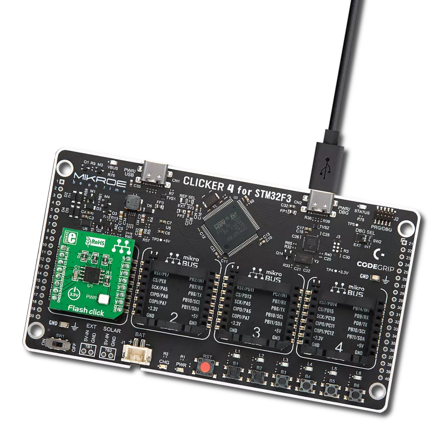
Fusion for Tiva v8
Compiler
NECTO Studio
MCU
TM4C123GH6PZ
Discover a new level of memory performance and security with this SPI serial flash memory solution
A
A
Hardware Overview
How does it work?
Flash 9 Click is based on the W25Q02JV, a highly reliable serial Flash memory solution offering flexibility and performance well beyond ordinary Serial Flash devices from Winbond Electronics. The W25Q02JV represents a four 512Mb stack die where only one can be active at any given time to communicate with the external SPI controller. It supports linear addressing for the full 2Gb memory address range (continuously read accessible only into four separate 512Mb address memory segments). The W25Q02JV array is organized into 1,048,576 programmable pages of 256 bytes each, where up to 256 bytes can be programmed at a time. Pages of the W25Q02JV can be erased in groups of 16 (4KB sector erase), groups of 128 (32KB block erase), groups of 256 (64KB block erase), or the entire chip (chip erase). This IC has 32,768 erasable 4KB sectors and 2,048 erasable 64KB blocks, respectively.
The small 4KB sectors allow for greater flexibility in applications that require data and parameter storage. Also, it specifies a minimum of 100.000 endurance cycles with data retention of a minimum of 20 years, which gives the W25Q02JV the capability to handle unlimited reads/writes to the memory. Flash 9 Click communicates with MCU through a standard SPI interface that enables high clock speed, supporting the two most common SPI modes, SPI Mode 0 and 3. Alongside the internal software Reset sequence, this board has an active-low reset signal routed on the RST pin of the mikroBUS™ socket used to reset the W25Q02JV to the initial power-on state. When this signal is asserted low, any ongoing program/erase operation will be interrupted, and data corruption may happen (the device will not accept any command input). An additional feature of this Click board™
represents the configurable Write Protection function labeled as WP routed on the AN pin of the mikroBUS™ socket. The WP pin protects the entire memory and all registers from write operations and must be set to a low logic state to inhibit all the write operations. Besides, the Flash 9 Click also has an additional hold pin, labeled as HLD, and routed to the PWM pin of the mikroBUS™ socket, allowing the device to be paused while it’s still actively selected. This Click board™ can only be operated with a 3.3V logic voltage level. The board must perform appropriate logic voltage level conversion before using MCUs with different logic levels. However, the Click board™ comes equipped with a library containing functions and an example code that can be used as a reference for further development.


Features overview
Development board
Fusion for TIVA v8 is a development board specially designed for the needs of rapid development of embedded applications. It supports a wide range of microcontrollers, such as different 32-bit ARM® Cortex®-M based MCUs from Texas Instruments, regardless of their number of pins, and a broad set of unique functions, such as the first-ever embedded debugger/programmer over a WiFi network. The development board is well organized and designed so that the end-user has all the necessary elements, such as switches, buttons, indicators, connectors, and others, in one place. Thanks to innovative manufacturing technology, Fusion for TIVA v8 provides a fluid and immersive working experience, allowing access
anywhere and under any circumstances at any time. Each part of the Fusion for TIVA v8 development board contains the components necessary for the most efficient operation of the same board. An advanced integrated CODEGRIP programmer/debugger module offers many valuable programming/debugging options, including support for JTAG, SWD, and SWO Trace (Single Wire Output)), and seamless integration with the Mikroe software environment. Besides, it also includes a clean and regulated power supply module for the development board. It can use a wide range of external power sources, including a battery, an external 12V power supply, and a power source via the USB Type-C (USB-C) connector.
Communication options such as USB-UART, USB HOST/DEVICE, CAN (on the MCU card, if supported), and Ethernet is also included. In addition, it also has the well-established mikroBUS™ standard, a standardized socket for the MCU card (SiBRAIN standard), and two display options for the TFT board line of products and character-based LCD. Fusion for TIVA v8 is an integral part of the Mikroe ecosystem for rapid development. Natively supported by Mikroe software tools, it covers many aspects of prototyping and development thanks to a considerable number of different Click boards™ (over a thousand boards), the number of which is growing every day.

Microcontroller Overview
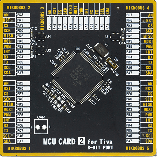
MCU Card / MCU
Type
8th Generation
Architecture
ARM Cortex-M4
MCU Memory (KB)
256
Silicon Vendor
Texas Instruments
Pin count
100
RAM (Bytes)
32768
Used MCU Pins
mikroBUS™ mapper
Take a closer look
Click board™ Schematic

Step by step
Project assembly

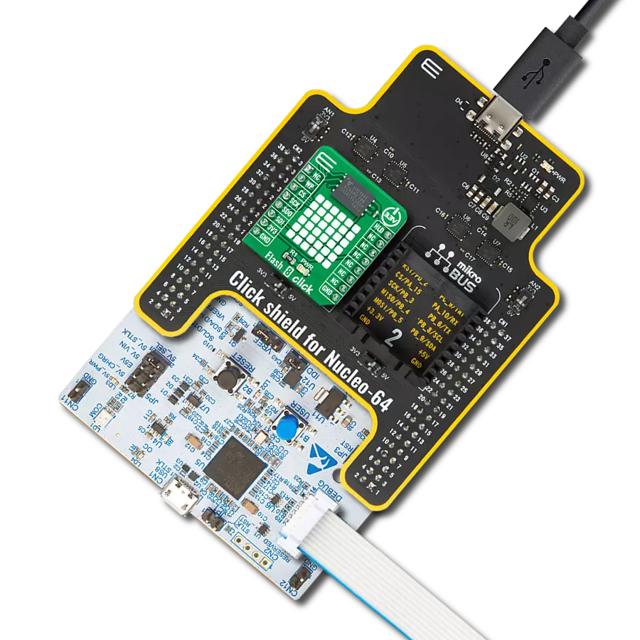
Start by selecting your development board and Click board™. Begin with the Fusion for Tiva v8 as your development board.


Track your results in real time
Application Output
1. Application Output - In Debug mode, the 'Application Output' window enables real-time data monitoring, offering direct insight into execution results. Ensure proper data display by configuring the environment correctly using the provided tutorial.

2. UART Terminal - Use the UART Terminal to monitor data transmission via a USB to UART converter, allowing direct communication between the Click board™ and your development system. Configure the baud rate and other serial settings according to your project's requirements to ensure proper functionality. For step-by-step setup instructions, refer to the provided tutorial.

3. Plot Output - The Plot feature offers a powerful way to visualize real-time sensor data, enabling trend analysis, debugging, and comparison of multiple data points. To set it up correctly, follow the provided tutorial, which includes a step-by-step example of using the Plot feature to display Click board™ readings. To use the Plot feature in your code, use the function: plot(*insert_graph_name*, variable_name);. This is a general format, and it is up to the user to replace 'insert_graph_name' with the actual graph name and 'variable_name' with the parameter to be displayed.

Software Support
Library Description
This library contains API for Flash 9 Click driver.
Key functions:
flash9_erase_memoryThis function erases the selected amount of memory that contains the selected address.flash9_memory_writeThis function writes a desired number of data bytes to the memory starting from the selected address.flash9_memory_read_fastThis function reads a desired number of data bytes from memory starting from the selected address performing the fast read command.
Open Source
Code example
The complete application code and a ready-to-use project are available through the NECTO Studio Package Manager for direct installation in the NECTO Studio. The application code can also be found on the MIKROE GitHub account.
/*!
 * @file main.c
 * @brief Flash9 Click example
 *
 * # Description
 * This example demonstrates the use of Flash 9 Click board by writing specified data to
 * the memory and reading it back.
 *
 * The demo application is composed of two sections :
 *
 * ## Application Init
 * Initializes the driver and performs the Click default configuration.
 *
 * ## Application Task
 * Erases the memory sector and then writes a desired number of data bytes to the memory
 * and verifies that it is written correctly by reading from the same memory location and
 * displaying the memory content on the USB UART.
 *
 * @author Stefan Filipovic
 *
 */

#include "board.h"
#include "log.h"
#include "flash9.h"

#define DEMO_TEXT_MESSAGE           "MikroE - Flash 9 Click board"
#define STARTING_ADDRESS            0x01234567ul

static flash9_t flash9;
static log_t logger;

void application_init ( void )
{
    log_cfg_t log_cfg;  /**< Logger config object. */
    flash9_cfg_t flash9_cfg;  /**< Click config object. */

    /**
     * Logger initialization.
     * Default baud rate: 115200
     * Default log level: LOG_LEVEL_DEBUG
     * @note If USB_UART_RX and USB_UART_TX
     * are defined as HAL_PIN_NC, you will
     * need to define them manually for log to work.
     * See @b LOG_MAP_USB_UART macro definition for detailed explanation.
     */
    LOG_MAP_USB_UART( log_cfg );
    log_init( &logger, &log_cfg );
    log_info( &logger, " Application Init " );

    // Click initialization.
    flash9_cfg_setup( &flash9_cfg );
    FLASH9_MAP_MIKROBUS( flash9_cfg, MIKROBUS_1 );
    if ( SPI_MASTER_ERROR == flash9_init( &flash9, &flash9_cfg ) )
    {
        log_error( &logger, " Communication init." );
        for ( ; ; );
    }

    if ( FLASH9_ERROR == flash9_default_cfg ( &flash9 ) )
    {
        log_error( &logger, " Default configuration." );
        for ( ; ; );
    }

    log_info( &logger, " Application Task " );
}

void application_task ( void )
{
    uint8_t data_buf[ 128 ] = { 0 };
    if ( FLASH9_OK == flash9_erase_memory ( &flash9, FLASH9_CMD_SECTOR_ERASE_WITH_4BYTE_ADDRESS,
                                            STARTING_ADDRESS ) )
    {
        log_printf ( &logger, "Sector from address 0x%.8LX has been erased!\r\n", STARTING_ADDRESS );
    }
    Delay_ms ( 500 );

    if ( FLASH9_OK == flash9_memory_write ( &flash9, STARTING_ADDRESS, DEMO_TEXT_MESSAGE,
                                            strlen ( DEMO_TEXT_MESSAGE ) ) )
    {
        log_printf ( &logger, "Data written to address 0x%.8LX: \"%s\"\r\n", STARTING_ADDRESS,
                                                                  ( char * ) DEMO_TEXT_MESSAGE );
    }
    Delay_ms ( 500 );

    if ( FLASH9_OK == flash9_memory_read_fast ( &flash9, STARTING_ADDRESS, data_buf,
                                                strlen ( DEMO_TEXT_MESSAGE ) ) )
    {
        log_printf ( &logger, "Data read from address 0x%.8LX: \"%s\"\r\n\n", STARTING_ADDRESS,
                                                                              data_buf );
    }
    Delay_ms ( 1000 );
    Delay_ms ( 1000 );
}

int main ( void )
{
    /* Do not remove this line or clock might not be set correctly. */
    #ifdef PREINIT_SUPPORTED
    preinit();
    #endif

    application_init( );

    for ( ; ; )
    {
        application_task( );
    }

    return 0;
}

// ------------------------------------------------------------------------ END