Ignite your power with TPS55332-Q1 and MK64FN1M0VDC12
Experience the boost

Published Jul 20, 2023
Click board™
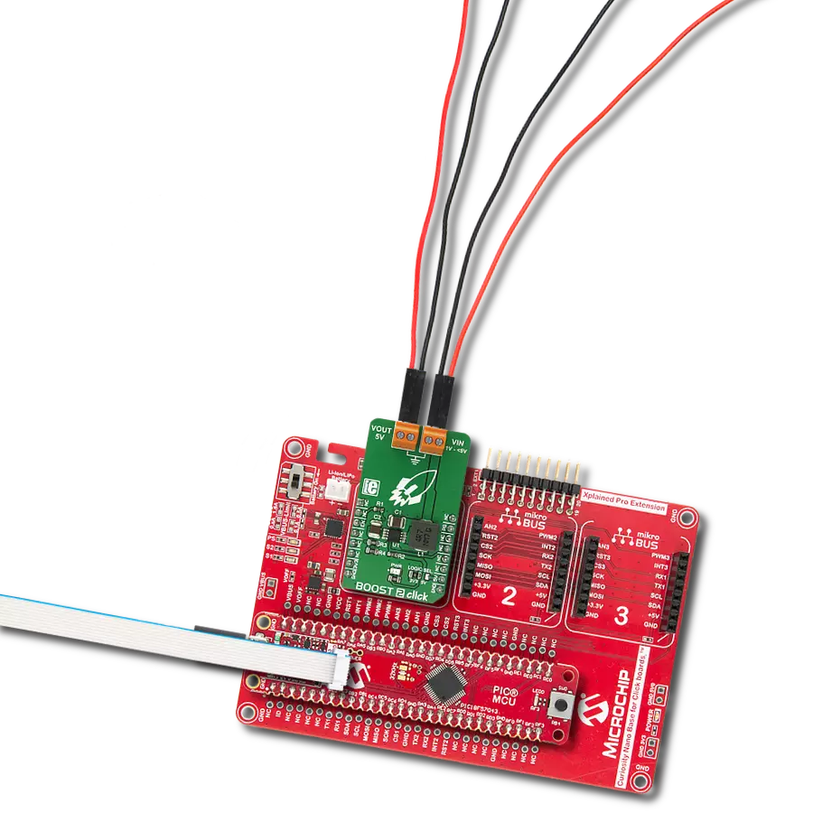
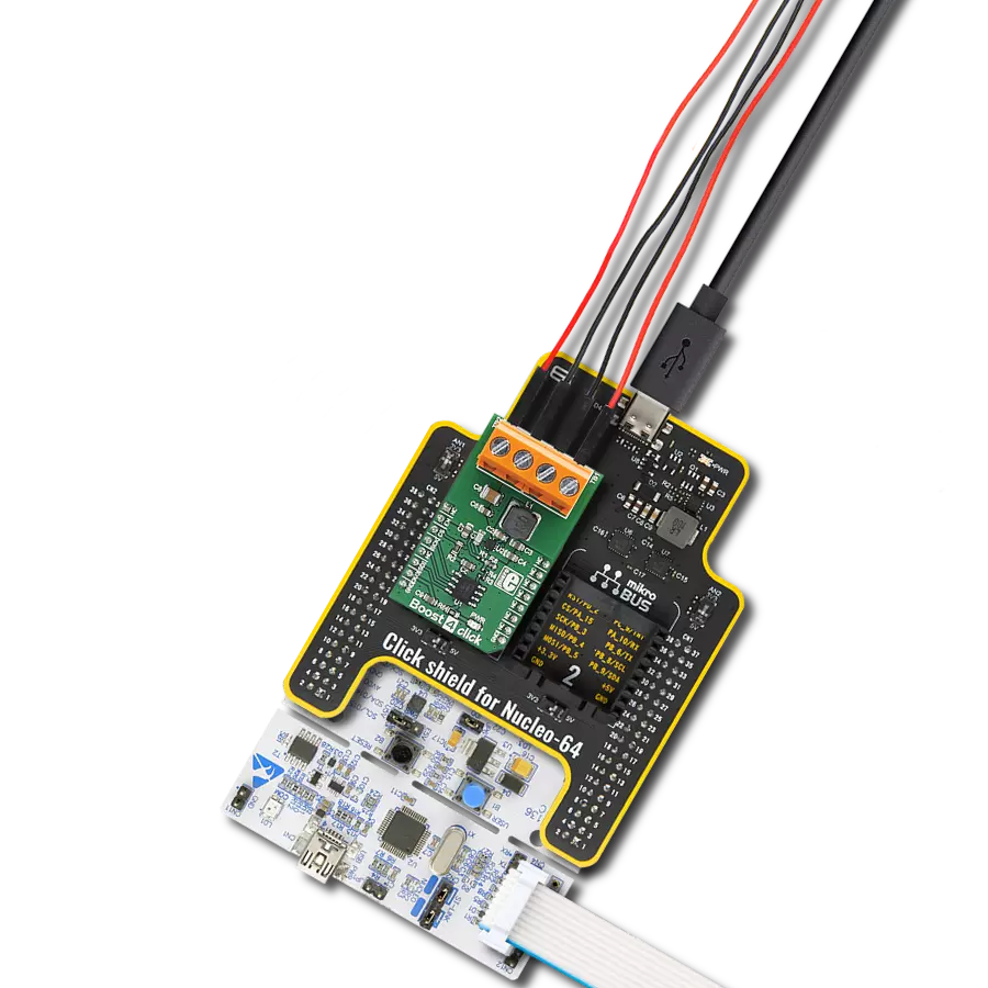
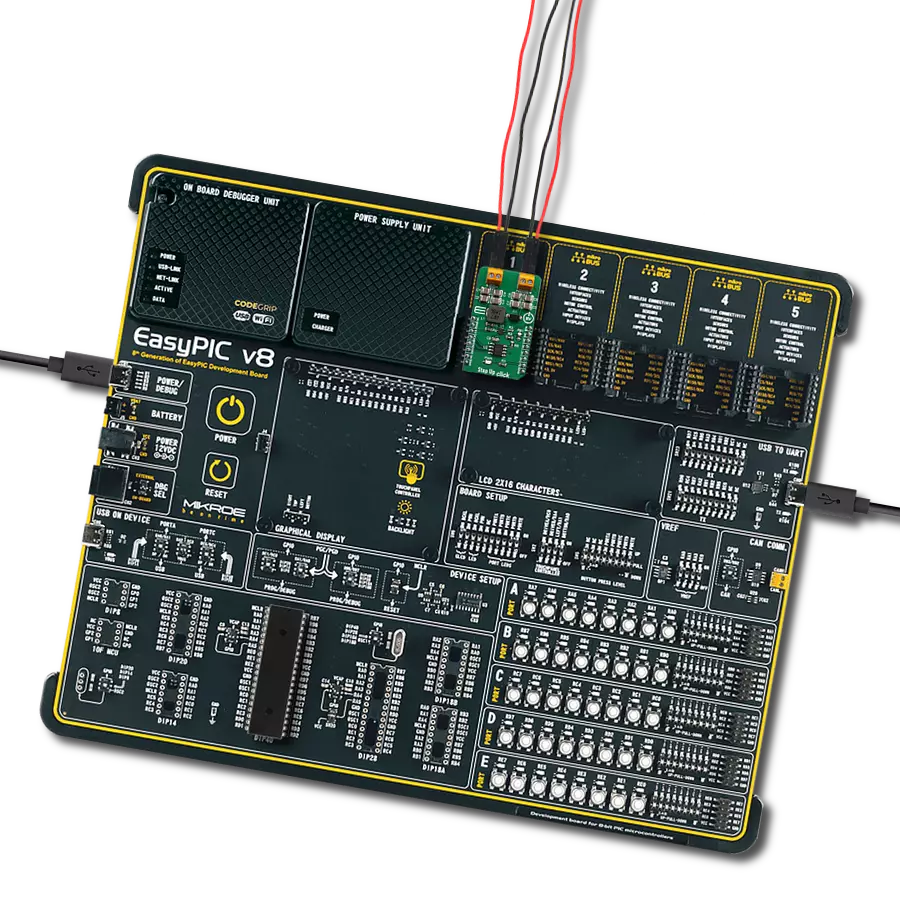
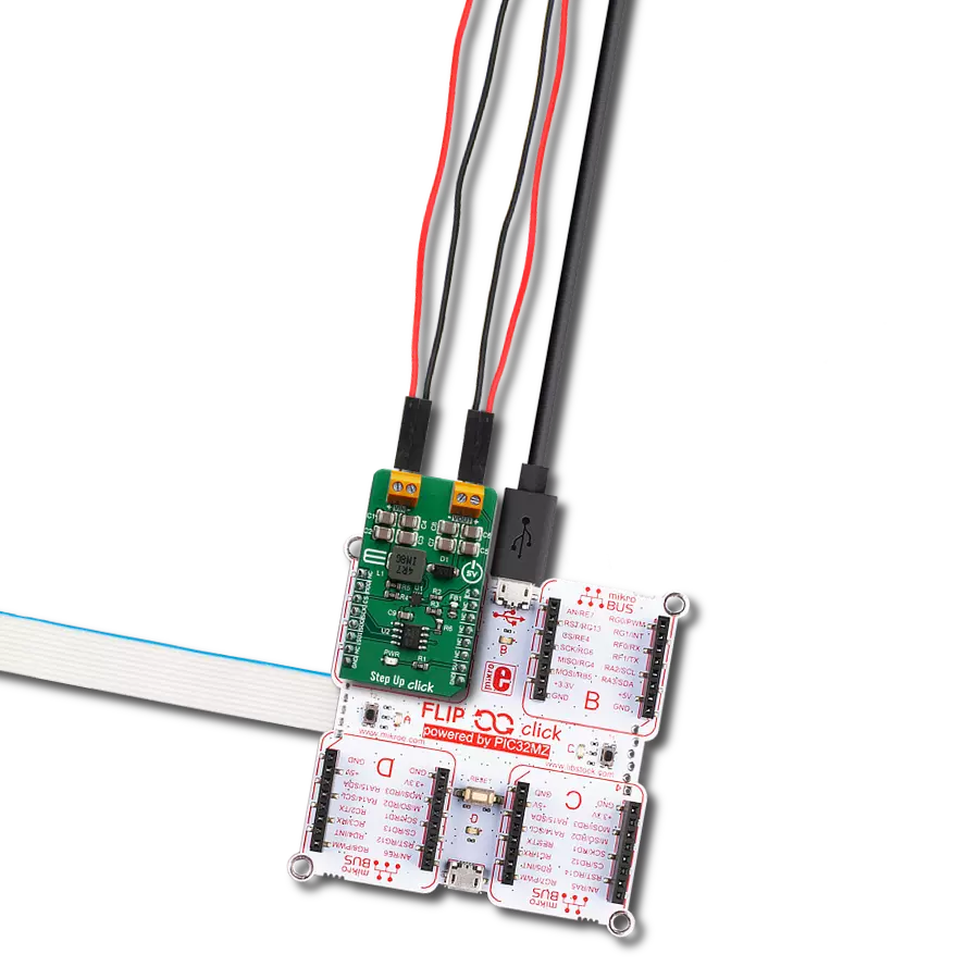
Boost 6 Click
Dev. board
Clicker 2 for Kinetis
Compiler
NECTO Studio
MCU
MK64FN1M0VDC12
Empower your circuits to soar with our state-of-the-art voltage booster!
A
A
Hardware Overview
How does it work?
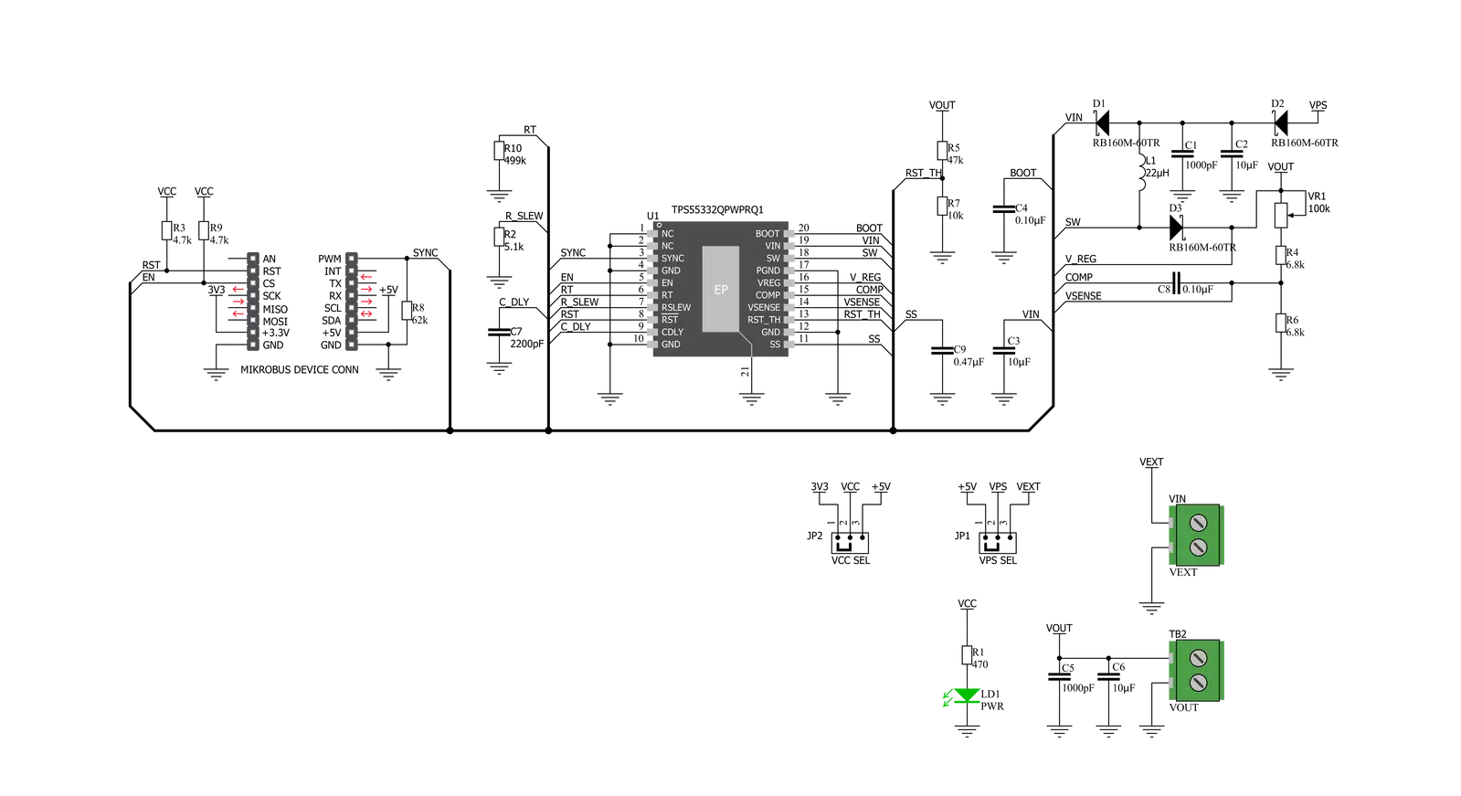
Boost 6 Click is based on the TPS55332-Q1, the monolithic high-voltage switching regulator from Texas Instruments. It is important to state that it operates as a step-up (boost) converter. The feedback concept is voltage mode control using the VSENSE terminal with a cycle-by-cycle current limit. The voltage supervisory function for power-on-rest during system power-on monitoring the output voltage, and once this has exceeded the threshold set by RST_TH, a delay of 1.0 ms/nF (based on the capacitor value on the Cdly terminal) is invoked before the RST line is released high. The output is sensed through an external resistor divider and compared with an internal reference voltage. The value of the adjustable output voltage in boost mode is selectable between VIN × 1.05 to 50 V if the minimum ON time (ton) and minimum OFF times are NOT violated by choosing the external resistors. The internal reference voltage Vref has a ±1.5% tolerance. The potentiometer featured on the Boost 6 click can change the feedback, thus influencing a change in the output voltage.
This makes the Click extremely practical because you can get the full voltage range with a simple turn of the potentiometer. Once the internal circuits have stabilized with a minimum input supply of 3.6V, the system can have an input voltage range from 1.5V to 40V to maintain a fixed boost output voltage. Over-current protection is implemented by sensing the current through the NMOS switch FET. The sensed current is then compared to a current reference level representing the over-current threshold limit. The over-current indicator is set to true if the sensed current exceeds the over-current threshold limit. The system ignores the over-current indicator for the leading edge blanking time at the beginning of each cycle to avoid any turn-on noise glitches. The oscillator frequency is selectable by means of a resistor placed at the RT pin. The switching frequency (ƒsw) can be set at 80kHz to 2.2MHz. The power-on reset output is asserted low until the output voltage exceeds the programmed Vreg_RST voltage threshold and the reset delay timer has expired. Additionally, whenever the
Enable pin is low or open, RST is immediately asserted low regardless of the output voltage. There is a reset de-glitch timer to prevent a reset from being invoked due to short negative transients on the output line. The TPS55332-Q1 device is designed to operate from an input voltage of up to 40 V. Ensure that the input supply is well-regulated and can protect itself from overheating with an internal thermal shutdown circuit. The MOSFET is turned off if the junction temperature exceeds the thermal shutdown trip point. The device is restarted under the control of the slow start circuit automatically when the junction temperature drops below the thermal shutdown hysteresis trip point. This Click board™ can operate with either 3.3V or 5V logic voltage levels selected via the VCC SEL jumper. This way, both 3.3V and 5V capable MCUs can use the communication lines properly. However, the Click board™ comes equipped with a library containing easy-to-use functions and an example code that can be used, as a reference, for further development.

Features overview
Development board
Clicker 2 for Kinetis is a compact starter development board that brings the flexibility of add-on Click boards™ to your favorite microcontroller, making it a perfect starter kit for implementing your ideas. It comes with an onboard 32-bit ARM Cortex-M4F microcontroller, the MK64FN1M0VDC12 from NXP Semiconductors, two mikroBUS™ sockets for Click board™ connectivity, a USB connector, LED indicators, buttons, a JTAG programmer connector, and two 26-pin headers for interfacing with external electronics. Its compact design with clear and easily recognizable silkscreen markings allows you to build gadgets with unique functionalities and
features quickly. Each part of the Clicker 2 for Kinetis development kit contains the components necessary for the most efficient operation of the same board. In addition to the possibility of choosing the Clicker 2 for Kinetis programming method, using a USB HID mikroBootloader or an external mikroProg connector for Kinetis programmer, the Clicker 2 board also includes a clean and regulated power supply module for the development kit. It provides two ways of board-powering; through the USB Micro-B cable, where onboard voltage regulators provide the appropriate voltage levels to each component on the board, or
using a Li-Polymer battery via an onboard battery connector. All communication methods that mikroBUS™ itself supports are on this board, including the well-established mikroBUS™ socket, reset button, and several user-configurable buttons and LED indicators. Clicker 2 for Kinetis is an integral part of the Mikroe ecosystem, allowing you to create a new application in minutes. Natively supported by Mikroe software tools, it covers many aspects of prototyping thanks to a considerable number of different Click boards™ (over a thousand boards), the number of which is growing every day.

Microcontroller Overview
MCU Card / MCU

Architecture
ARM Cortex-M4
MCU Memory (KB)
1024
Silicon Vendor
NXP
Pin count
121
RAM (Bytes)
262144
Used MCU Pins
mikroBUS™ mapper
Take a closer look
Click board™ Schematic
Step by step
Project assembly

Start by selecting your development board and Click board™. Begin with the Clicker 2 for Kinetis as your development board.


Track your results in real time
Application Output
1. Application Output - In Debug mode, the 'Application Output' window enables real-time data monitoring, offering direct insight into execution results. Ensure proper data display by configuring the environment correctly using the provided tutorial.

2. UART Terminal - Use the UART Terminal to monitor data transmission via a USB to UART converter, allowing direct communication between the Click board™ and your development system. Configure the baud rate and other serial settings according to your project's requirements to ensure proper functionality. For step-by-step setup instructions, refer to the provided tutorial.

3. Plot Output - The Plot feature offers a powerful way to visualize real-time sensor data, enabling trend analysis, debugging, and comparison of multiple data points. To set it up correctly, follow the provided tutorial, which includes a step-by-step example of using the Plot feature to display Click board™ readings. To use the Plot feature in your code, use the function: plot(*insert_graph_name*, variable_name);. This is a general format, and it is up to the user to replace 'insert_graph_name' with the actual graph name and 'variable_name' with the parameter to be displayed.

Software Support
Library Description
This library contains API for Boost 6 Click driver.
Key functions:
boost6_hw_reset- This function hardware reset the TPS55332-Q1boost6_power_off- This function powers OFF the TPS55332-Q1boost6_power_on- This function powers ON the TPS55332-Q1
Open Source
Code example
The complete application code and a ready-to-use project are available through the NECTO Studio Package Manager for direct installation in the NECTO Studio. The application code can also be found on the MIKROE GitHub account.
/*!
 * \file
 * \brief Boost 6 Click example
 *
 * # Description
 * This app enable or disable monolithic high-voltage switching regulator.
 *
 * The demo application is composed of two sections :
 *
 * ## Application Init
 * Initializes device.
 *
 * ## Application Task
 * This is an example which demonstrates the use of Boost 6 Click board.
 * Enable device 5000ms and disable device 5000ms.
 *
 * \author MikroE Team
 *
 */
// ------------------------------------------------------------------- INCLUDES

#include "board.h"
#include "log.h"
#include "boost6.h"

// ------------------------------------------------------------------ VARIABLES

static boost6_t boost6;
static log_t logger;

// ------------------------------------------------------ APPLICATION FUNCTIONS

void application_init ( void )
{
    log_cfg_t log_cfg;
    boost6_cfg_t cfg;

    /**
     * Logger initialization.
     * Default baud rate: 115200
     * Default log level: LOG_LEVEL_DEBUG
     * @note If USB_UART_RX and USB_UART_TX
     * are defined as HAL_PIN_NC, you will
     * need to define them manually for log to work.
     * See @b LOG_MAP_USB_UART macro definition for detailed explanation.
     */
    LOG_MAP_USB_UART( log_cfg );
    log_init( &logger, &log_cfg );
    log_info( &logger, "---- Application Init ----\r\n" );

    //  Click initialization.

    boost6_cfg_setup( &cfg );
    BOOST6_MAP_MIKROBUS( cfg, MIKROBUS_1 );
    boost6_init( &boost6, &cfg );

    log_printf( &logger, "-----------------\r\n" );
    log_printf( &logger, "  Boost 6 Click  \r\n" );
    log_printf( &logger, "-----------------\r\n" );

    log_printf( &logger, "-----------------\r\n" );
    log_printf( &logger, " Hardware  Reset \r\n" );
    log_printf( &logger, "-----------------\r\n" );
    boost6_hw_reset ( &boost6 );
    Delay_100ms( );

    boost6_power_off(  &boost6  );
    log_printf( &logger, "     Disable     \r\n" );
    log_printf( &logger, "-----------------\r\n" );
    Delay_100ms( );
}

void application_task ( void )
{
    boost6_power_on( &boost6 );
    log_printf( &logger, "     Enable      \r\n" );
    log_printf( &logger, "-----------------\r\n" );

    Delay_ms ( 1000 );
    Delay_ms ( 1000 );
    Delay_ms ( 1000 );
    Delay_ms ( 1000 );
    Delay_ms ( 1000 );

    boost6_power_off(  &boost6  );
    log_printf( &logger, "     Disable     \r\n" );
    log_printf( &logger, "-----------------\r\n" );

    Delay_ms ( 1000 );
    Delay_ms ( 1000 );
    Delay_ms ( 1000 );
    Delay_ms ( 1000 );
    Delay_ms ( 1000 );
}

int main ( void )
{
    /* Do not remove this line or clock might not be set correctly. */
    #ifdef PREINIT_SUPPORTED
    preinit();
    #endif

    application_init( );

    for ( ; ; )
    {
        application_task( );
    }

    return 0;
}

// ------------------------------------------------------------------------ END