Unlock balanced power with TPS65131 and PIC18LF45K50
From minus to plus
Published Jul 19, 2023
Click board™
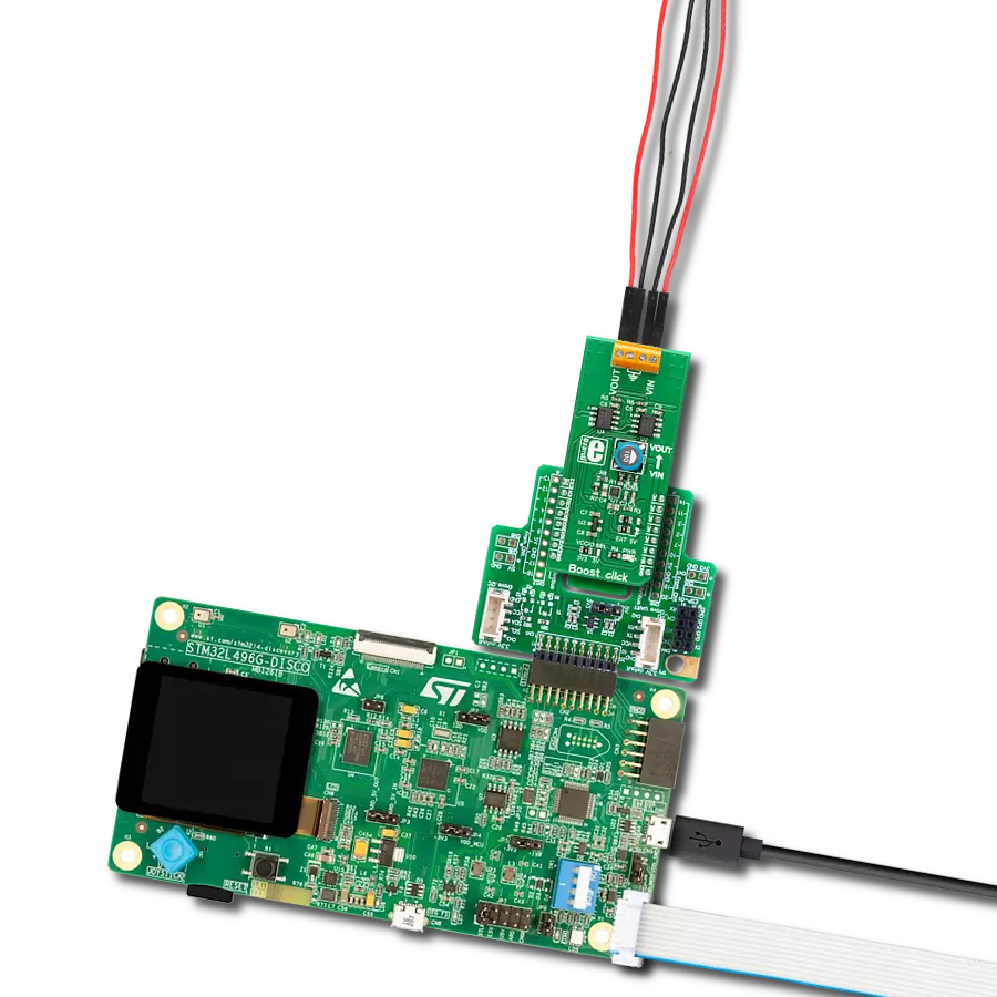
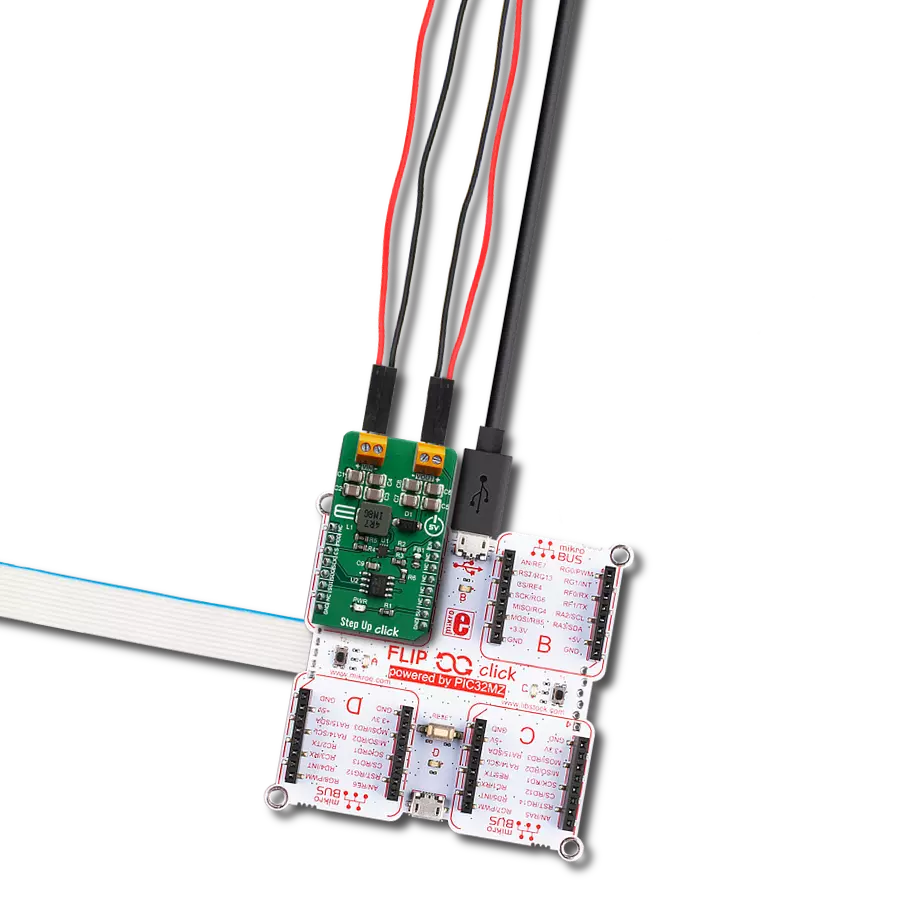
Boost-INV 2 Click
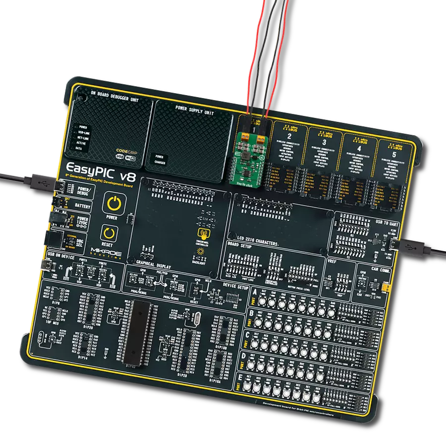
Dev. board
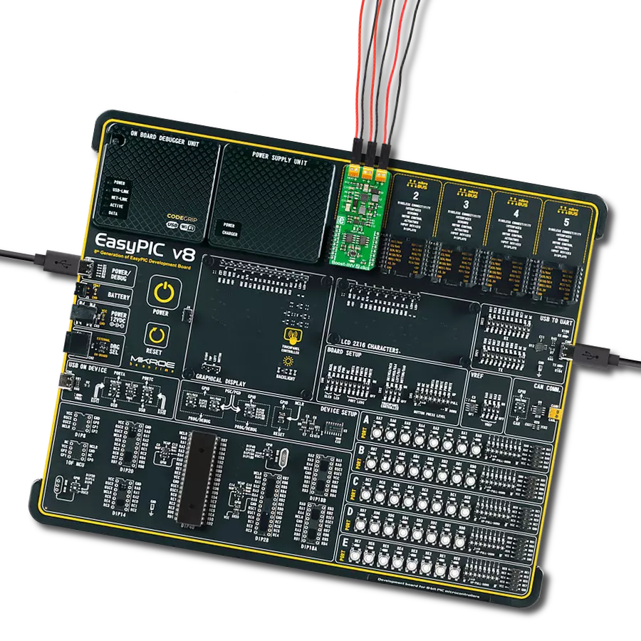
EasyPIC v8
Compiler
NECTO Studio
MCU
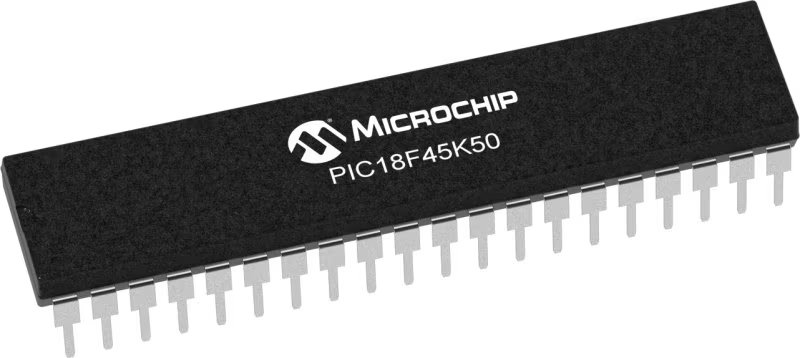
PIC18LF45K50
Embrace the symmetry of power with our dual-polarity voltage conversion solution
A
A
Hardware Overview
How does it work?
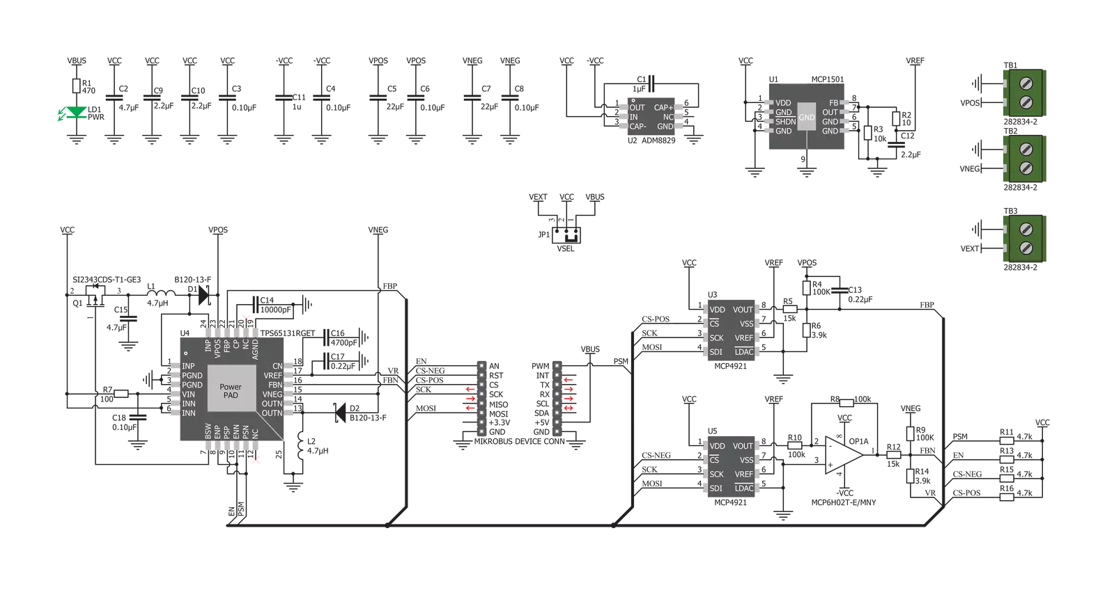
Boost-INV 2 Click is based on the TPS65131, a positive and negative output DC/DC converter from Texas Instruments. Two D/A converters are connected to the positive and negative voltage feedback loop of the TPS65131. The positive and the negative loops are fed into the internal error amplifiers, which compare the feedback voltage with the internal references. They change the duty cycle of the output switching sections to compensate for the differences (errors), affecting the output voltage that way. Incorporating a D/A converter into the feedback loop allows programmed "errors" to be introduced into the loop, allowing control over the output voltage. The TPS65131 IC uses the fixed frequency PWM signal to switch output stages. The internal current limit is about 1950mA for both the inverting and boost converter. The output voltage is clean while running in the continuous conduction mode, with no significant ripple and noise. The complete disconnect of both inverting and boosting converter stages allows no source current to flow through the converter while it is unpowered. This prevents battery draining, allowing the device to use the battery power and providing a split-rail power supply for various applications. Two D/A converters (DAC) labeled as MCP4291, 12-Bit DACs with the SPI Interface by Microchip, are used in feedback loops. One of the DACs is connected
to the MCP6H02 op-amp, configured as the inverting unity gain amplifier. It inverts the polarity of the DAC signal. The feedback voltage of the inverting converter can vary from 0V (Vref) to -15V. Therefore, the DAC signal, which commonly ranges from 0 to +VREF, needs to be inverted. For the boost converter, there is no need to invert the DAC, so its voltage goes up to +VREF. There are two separate CS pins (Chip Select) for these DACs, so both can be programmed independently. Those Chip Select pins are routed to the RST and CS pins of the mikroBUS™ and are labeled as CSN for the negative voltage-controlling DAC and CSP for the positive voltage-controlling DAC. Two more auxiliary ICs are used on the Boost-INV 2 click. One IC is the ADM8829, a switched-capacitor voltage inverter that provides a negative supply voltage for the inverting op-amp. The other IC is the MCP1501, a high-precision buffered voltage reference required for the DACs (4.096 V). The TPS65131 converter IC can be operated in the Power Saving mode. This is very useful for low currents because the device will power itself down as long as the voltage across the output stays above the internally set threshold. When the voltage drops under this threshold, the converter powers up produces several switching pulses that recover the nominal voltage value across the load, and power down again. Depending on the connected
load, it will take more or less time to drain the charge from the inductor. Unlike the normal mode, which operates in the continuous-conduction mode (CCM), the power-saving mode allows the converter to switch between CCM and DCM (discontinuous-conduction) modes. The Click board™ has its PWM pin routed to the PSP and PSN pins of the TPS65131 IC, and the HIGH logic level on this pin will put the IC into the Power Saving mode. The PWM pin of the mikroBUS™ is labeled as the PSM on this Click board™. When the ENP and ENN pins of the TPS65131 IC are at the LOW logic level, the device is completely powered down, disconnecting the loads described above and preventing current leakage through the passive elements of the circuit. These pins are routed to the AN pin of the mikroBUS™ and labeled as EN, allowing the host MCU to control the operation of the Click board™ By default, the input voltage is taken from the mikroBUS™ +5V power rail. An onboard VIN SEL jumper allows selection between the +5V from the mikroBUS™ or an external power supply connected to the screw terminal input, labeled as VEXT. The remaining two screw terminals are negative and positive voltage outputs labeled V- and V+. All three screw terminals share a common GND.

Features overview
Development board
EasyPIC v8 is a development board specially designed for the needs of rapid development of embedded applications. It supports many high pin count 8-bit PIC microcontrollers from Microchip, regardless of their number of pins, and a broad set of unique functions, such as the first-ever embedded debugger/programmer. The development board is well organized and designed so that the end-user has all the necessary elements, such as switches, buttons, indicators, connectors, and others, in one place. Thanks to innovative manufacturing technology, EasyPIC v8 provides a fluid and immersive working experience, allowing access anywhere and under any
circumstances at any time. Each part of the EasyPIC v8 development board contains the components necessary for the most efficient operation of the same board. In addition to the advanced integrated CODEGRIP programmer/debugger module, which offers many valuable programming/debugging options and seamless integration with the Mikroe software environment, the board also includes a clean and regulated power supply module for the development board. It can use a wide range of external power sources, including a battery, an external 12V power supply, and a power source via the USB Type-C (USB-C) connector.
Communication options such as USB-UART, USB DEVICE, and CAN are also included, including the well-established mikroBUS™ standard, two display options (graphical and character-based LCD), and several different DIP sockets. These sockets cover a wide range of 8-bit PIC MCUs, from the smallest PIC MCU devices with only eight up to forty pins. EasyPIC v8 is an integral part of the Mikroe ecosystem for rapid development. Natively supported by Mikroe software tools, it covers many aspects of prototyping and development thanks to a considerable number of different Click boards™ (over a thousand boards), the number of which is growing every day.

Microcontroller Overview
MCU Card / MCU
Architecture
PIC
MCU Memory (KB)
32
Silicon Vendor
Microchip
Pin count
40
RAM (Bytes)
2048
Used MCU Pins
mikroBUS™ mapper
Take a closer look
Click board™ Schematic
Step by step
Project assembly

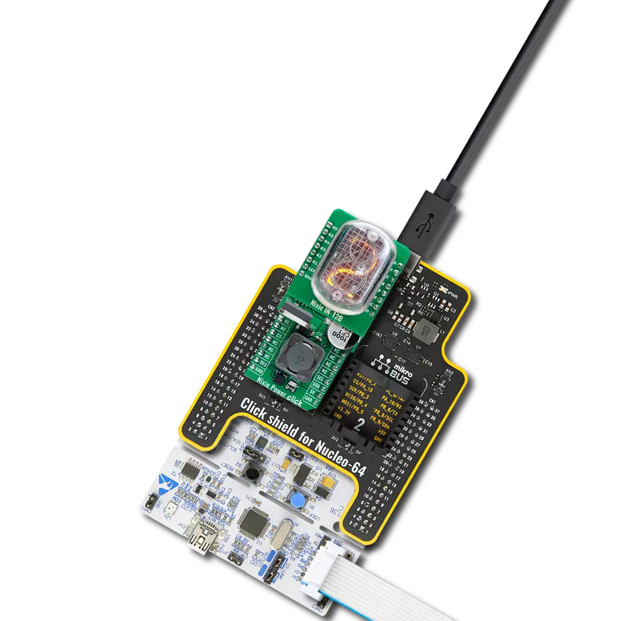
Start by selecting your development board and Click board™. Begin with the EasyPIC v8 as your development board.


Track your results in real time
Application Output
1. Application Output - In Debug mode, the 'Application Output' window enables real-time data monitoring, offering direct insight into execution results. Ensure proper data display by configuring the environment correctly using the provided tutorial.

2. UART Terminal - Use the UART Terminal to monitor data transmission via a USB to UART converter, allowing direct communication between the Click board™ and your development system. Configure the baud rate and other serial settings according to your project's requirements to ensure proper functionality. For step-by-step setup instructions, refer to the provided tutorial.

3. Plot Output - The Plot feature offers a powerful way to visualize real-time sensor data, enabling trend analysis, debugging, and comparison of multiple data points. To set it up correctly, follow the provided tutorial, which includes a step-by-step example of using the Plot feature to display Click board™ readings. To use the Plot feature in your code, use the function: plot(*insert_graph_name*, variable_name);. This is a general format, and it is up to the user to replace 'insert_graph_name' with the actual graph name and 'variable_name' with the parameter to be displayed.

Software Support
Library Description
This library contains API for Boost-INV 2 Click driver.
Key functions:
boostinv2_set_positive_voltage- Functions for set positive output voltageboostinv2_set_negative_voltage- Functions for set negative output voltageboostinv2_generic_transfer- Generic transfer function
Open Source
Code example
The complete application code and a ready-to-use project are available through the NECTO Studio Package Manager for direct installation in the NECTO Studio. The application code can also be found on the MIKROE GitHub account.
/*!
 * \file
 * \brief boostinv2 Click example
 *
 * # Description
 * First increse positiv voltage by 2V every 3 seconda, then
 * decrese negative value for -2v every 3 seconds.
 *
 * The demo application is composed of two sections :
 *
 * ## Application Init
 * Initializes Driver init and enable chip
 *
 * ## Application Task
 * Changes the positive and negative output voltage.
 * Positive output voltage goes from 5V to 15V.
 * Negative output voltage goes from -5V to -15V
 *
 * \author MikroE Team
 *
 */
// ------------------------------------------------------------------- INCLUDES

#include "board.h"
#include "log.h"
#include "boostinv2.h"

// ------------------------------------------------------------------ VARIABLES

static boostinv2_t boostinv2;
static log_t logger;

// ------------------------------------------------------ APPLICATION FUNCTIONS

void application_init ( void )
{
    log_cfg_t log_cfg;
    boostinv2_cfg_t cfg;

    /**
     * Logger initialization.
     * Default baud rate: 115200
     * Default log level: LOG_LEVEL_DEBUG
     * @note If USB_UART_RX and USB_UART_TX
     * are defined as HAL_PIN_NC, you will
     * need to define them manually for log to work.
     * See @b LOG_MAP_USB_UART macro definition for detailed explanation.
     */
    LOG_MAP_USB_UART( log_cfg );
    log_init( &logger, &log_cfg );
    log_info( &logger, "---- Application Init ----" );

    //  Click initialization.

    boostinv2_cfg_setup( &cfg );
    BOOSTONV2_MAP_MIKROBUS( cfg, MIKROBUS_1 );
    boostinv2_init( &boostinv2, &cfg );

    boostinv2_enable( &boostinv2 );
}

void application_task ( void )
{
     // Positive output voltage
     log_printf( &logger, "VOUT = 6V\r\n");
     boostinv2_set_positive_voltage( &boostinv2, BOOSTINV2_POS_VOUT_6V );
     Delay_ms ( 1000 );
     Delay_ms ( 1000 );
     Delay_ms ( 1000 );
     log_printf( &logger, "VOUT = 8V\r\n");
     boostinv2_set_positive_voltage( &boostinv2, BOOSTINV2_POS_VOUT_8V );
     Delay_ms ( 1000 );
     Delay_ms ( 1000 );
     Delay_ms ( 1000 );
     log_printf( &logger, "VOUT = 12V\r\n");
     boostinv2_set_positive_voltage( &boostinv2, BOOSTINV2_POS_VOUT_12V );
     Delay_ms ( 1000 );
     Delay_ms ( 1000 );
     Delay_ms ( 1000 );
     log_printf( &logger, "VOUT = 14V\r\n");
     boostinv2_set_positive_voltage( &boostinv2, BOOSTINV2_POS_VOUT_14V );
     Delay_ms ( 1000 );
     Delay_ms ( 1000 );
     Delay_ms ( 1000 );
     log_printf( &logger, "VOUT = 12V\r\n");
     boostinv2_set_positive_voltage( &boostinv2, BOOSTINV2_POS_VOUT_12V );
     Delay_ms ( 1000 );
     Delay_ms ( 1000 );
     Delay_ms ( 1000 );
     log_printf( &logger, "VOUT = 8V\r\n");
     boostinv2_set_positive_voltage( &boostinv2, BOOSTINV2_POS_VOUT_8V );
     Delay_ms ( 1000 );
     Delay_ms ( 1000 );
     Delay_ms ( 1000 );

     // Negative output voltage

     log_printf( &logger, "VOUT = -5V\r\n");
     boostinv2_set_negative_voltage( &boostinv2, BOOSTINV2_NEG_VOUT_5V );
     Delay_ms ( 1000 );
     Delay_ms ( 1000 );
     Delay_ms ( 1000 );
     log_printf( &logger, "VOUT = -7V\r\n");
     boostinv2_set_negative_voltage( &boostinv2, BOOSTINV2_NEG_VOUT_7V );
     Delay_ms ( 1000 );
     Delay_ms ( 1000 );
     Delay_ms ( 1000 );
     log_printf( &logger, "VOUT = -13V\r\n");
     boostinv2_set_negative_voltage( &boostinv2, BOOSTINV2_NEG_VOUT_13V );
     Delay_ms ( 1000 );
     Delay_ms ( 1000 );
     Delay_ms ( 1000 );
     log_printf( &logger, "VOUT = -7V\r\n");
     boostinv2_set_negative_voltage( &boostinv2, BOOSTINV2_NEG_VOUT_7V );
     Delay_ms ( 1000 );
     Delay_ms ( 1000 );
     Delay_ms ( 1000 );
}

int main ( void )
{
    /* Do not remove this line or clock might not be set correctly. */
    #ifdef PREINIT_SUPPORTED
    preinit();
    #endif

    application_init( );

    for ( ; ; )
    {
        application_task( );
    }

    return 0;
}


// ------------------------------------------------------------------------ END