Process data swiftly thanks to the ANV32AA1WDK66 and PIC18F57Q43, no matter the task
Unlock unprecedented speed with our SRAM solution
Published Feb 13, 2024
Click board™
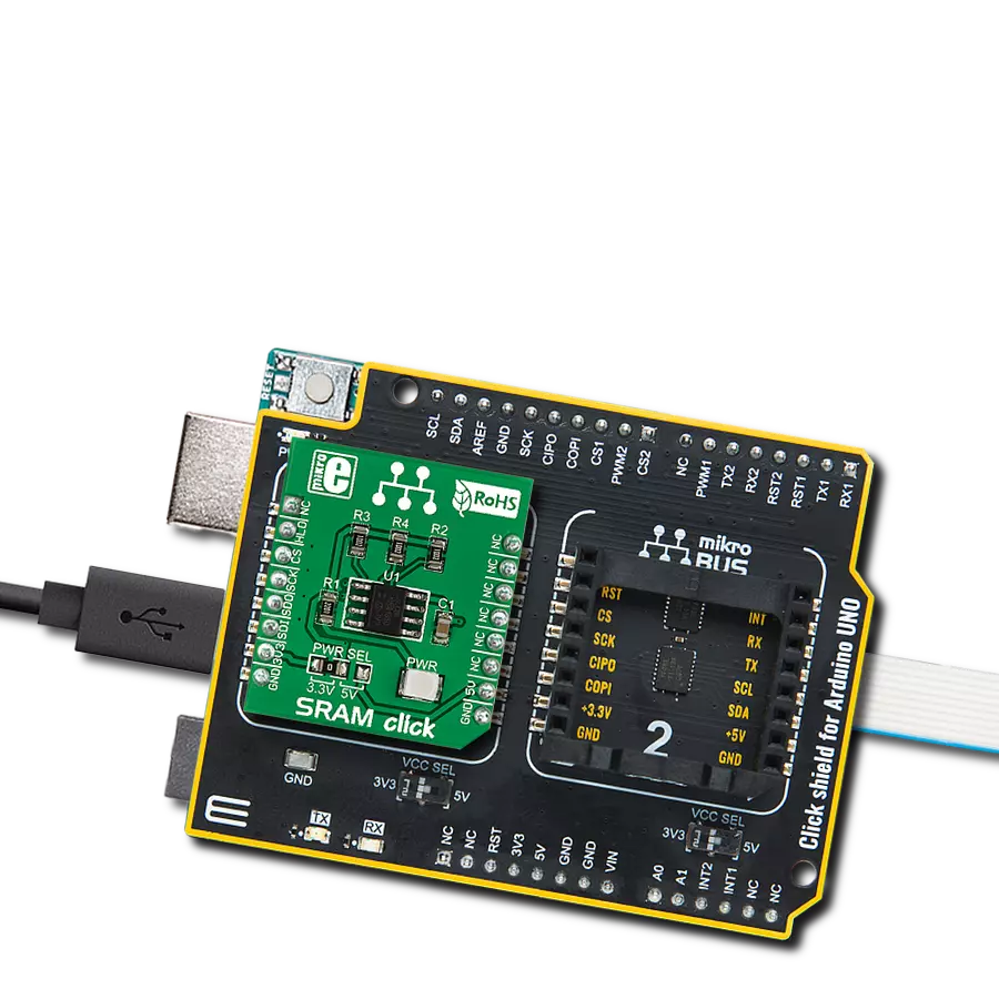
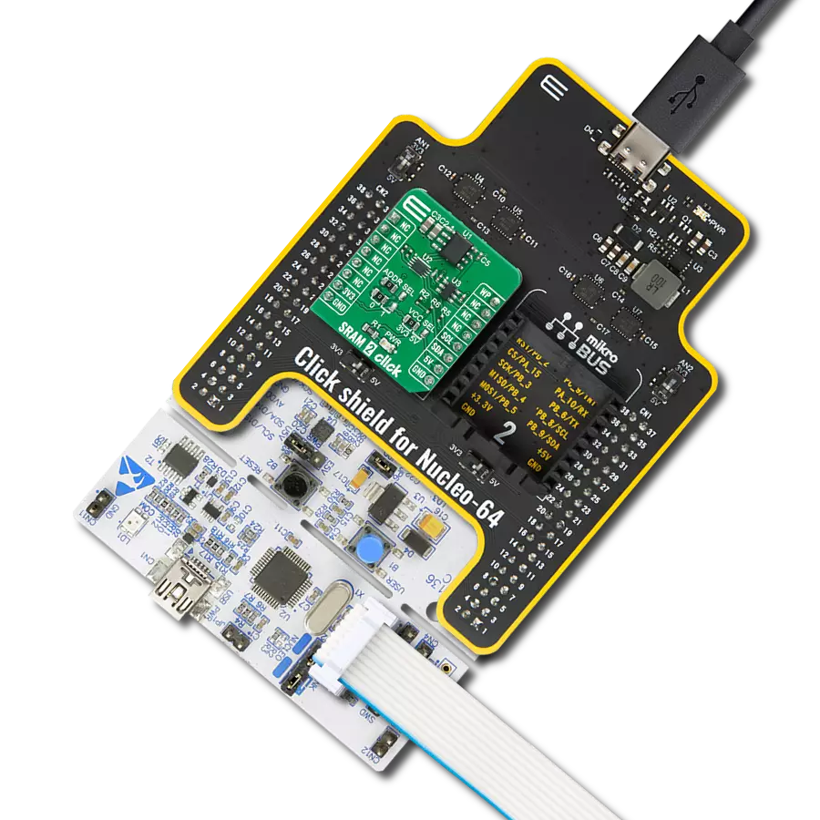
SRAM 3 Click
Dev. board
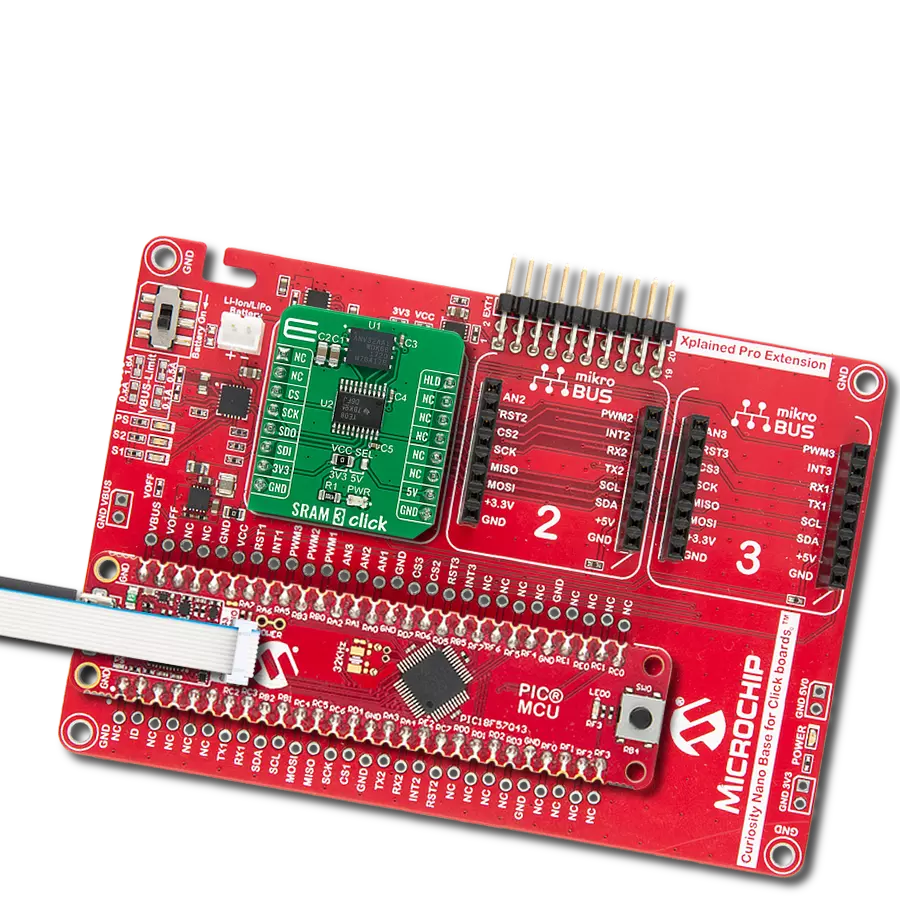
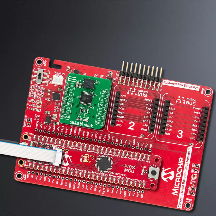
Curiosity Nano with PIC18F57Q43
Compiler
NECTO Studio
MCU
PIC18F57Q43
With our SRAM memory, you can trust in data integrity and fast access for critical operations
A
A
Hardware Overview
How does it work?
SRAM 3 Click is based on the ANV32AA1WDK66, a serial non-volatile SRAM with double memory architecture and SPI serial interface organized as 128k words of 8 bits each from Anvo-System Dresden. This memory has a silicon-oxide-nitride-oxide-silicon (SONOS) flash storage element included with each memory cell. In the case of an unforeseeable operating voltage drop below a defined value, the SONOS technology enables non-volatile data storage in less than 15ms. An integrated Power Down functionality of the SRAM 3 Click with a standby current of less than 1µA ensures low power consumption, with recovery time from Power-Down Mode typically of 60µs. This ANV32AA1WDK66 possesses unique safety features, such as Checksum Protected Memory Accesses (Secure READ and Secure WRITE instructions) and Time Monitoring that ensures a
high degree of reliability of this Click board™. Corrupt data cannot overwrite existing memory content; even valid data would not overwrite on a corrupted address. The SRAM 3 Click also provides some distinctive advantages of SRAMs, such as fast access times and unlimited write/read endurance. SRAM 3 Click incorporates an additional IC, the TXB0108PWR, an 8-bit bidirectional voltage level translator from Texas Instruments. This allows the Click board™ to be used with a much more extensive range of MCUs. At the same time, the TXB0108PWR protects the ANV32AA1WDK66 from the Electrostatic Discharges (ESD) up to ±15 kV, making SRAM 3 Click a very reliable embedded storage solution. The ANV32AA1WDK66 communicates with MCU using the standard SPI serial interface that supports modes 0 and 3 with a maximum
frequency of 66 MHz. It also possesses an additional HOLD function routed at the PWM pin of the mikroBUS™ socket labeled as HLD. This pin is used with the CS pin to select the device. When the device is selected, and a serial sequence is underway, an HLD pin can pause the serial communication with the host device without resetting the serial sequence. This Click board™ can operate with either 3.3V or 5V logic voltage levels selected via the VCC SEL jumper. This way, both 3.3V and 5V capable MCUs can use the communication lines properly. Also, this Click board™ comes equipped with a library containing easy-to-use functions and an example code that can be used as a reference for further development.

Features overview
Development board
PIC18F57Q43 Curiosity Nano evaluation kit is a cutting-edge hardware platform designed to evaluate microcontrollers within the PIC18-Q43 family. Central to its design is the inclusion of the powerful PIC18F57Q43 microcontroller (MCU), offering advanced functionalities and robust performance. Key features of this evaluation kit include a yellow user LED and a responsive
mechanical user switch, providing seamless interaction and testing. The provision for a 32.768kHz crystal footprint ensures precision timing capabilities. With an onboard debugger boasting a green power and status LED, programming and debugging become intuitive and efficient. Further enhancing its utility is the Virtual serial port (CDC) and a debug GPIO channel (DGI
GPIO), offering extensive connectivity options. Powered via USB, this kit boasts an adjustable target voltage feature facilitated by the MIC5353 LDO regulator, ensuring stable operation with an output voltage ranging from 1.8V to 5.1V, with a maximum output current of 500mA, subject to ambient temperature and voltage constraints.

Microcontroller Overview
MCU Card / MCU

Architecture
PIC
MCU Memory (KB)
128
Silicon Vendor
Microchip
Pin count
48
RAM (Bytes)
8196
You complete me!
Accessories
Curiosity Nano Base for Click boards is a versatile hardware extension platform created to streamline the integration between Curiosity Nano kits and extension boards, tailored explicitly for the mikroBUS™-standardized Click boards and Xplained Pro extension boards. This innovative base board (shield) offers seamless connectivity and expansion possibilities, simplifying experimentation and development. Key features include USB power compatibility from the Curiosity Nano kit, alongside an alternative external power input option for enhanced flexibility. The onboard Li-Ion/LiPo charger and management circuit ensure smooth operation for battery-powered applications, simplifying usage and management. Moreover, the base incorporates a fixed 3.3V PSU dedicated to target and mikroBUS™ power rails, alongside a fixed 5.0V boost converter catering to 5V power rails of mikroBUS™ sockets, providing stable power delivery for various connected devices.

Used MCU Pins
mikroBUS™ mapper
Take a closer look
Click board™ Schematic

Step by step
Project assembly

Start by selecting your development board and Click board™. Begin with the Curiosity Nano with PIC18F57Q43 as your development board.


Software Support
Library Description
This library contains API for SRAM 3 Click driver.
Key functions:
sram3_enable_write- This function is for enabling writing to memory, status register or user serial.sram3_disable_write- Function for disabling writing to memory, status register or user serial.sram3_protect_memory- Function which secures part of memory from writing.
Open Source
Code example
The complete application code and a ready-to-use project are available through the NECTO Studio Package Manager for direct installation in the NECTO Studio. The application code can also be found on the MIKROE GitHub account.
/*!
 * @file main.c
 * @brief SRAM3 Click example
 *
 * # Description
 * This is an example that shows the use of SRAM memory, using SRAM 3 Click. SRAM 3 Click is based on ANV32AA1W,
 * and ANV32AA1W is a 1Mb serial SRAM with a non-volatile SONOS storage element included with each memory cell,
 * organized as 128k words of 8 bits each. The devices are accessed by a high speed SPI-compatible bus.
 * Specifically in this example, we used the high-speed SPI communication characteristics to write data to a specific
 * registration address and read it.
 *
 * The demo application is composed of two sections :
 *
 * ## Application Init
 * Initialization SPI module, logger initalization and Click initialization.
 *
 * ## Application Task
 * First, we write the data to the registry address 0x00, and then we read the data from 0x00 address.
 *
 * @author Jelena Milosavljevic
 *
 */

#include "board.h"
#include "log.h"
#include "sram3.h"

static sram3_t sram3;
static log_t logger;
uint8_t buf[10] = { 'M','i','k','r','o','E', 0 };

void application_init ( void ) {
    log_cfg_t log_cfg;         /**< Logger config object. */
    sram3_cfg_t sram3_cfg;     /**< Click config object. */

    /**
     * Logger initialization.
     * Default baud rate: 115200
     * Default log level: LOG_LEVEL_DEBUG
     * @note If USB_UART_RX and USB_UART_TX
     * are defined as HAL_PIN_NC, you will
     * need to define them manually for log to work.
     * See @b LOG_MAP_USB_UART macro definition for detailed explanation.
     */
    LOG_MAP_USB_UART( log_cfg );
    log_init( &logger, &log_cfg );
    log_info( &logger, " Application Init " );

    // Click initialization.
    sram3_cfg_setup( &sram3_cfg );
    SRAM3_MAP_MIKROBUS( sram3_cfg, MIKROBUS_1 );
    err_t init_flag  = sram3_init( &sram3, &sram3_cfg );
    if ( SPI_MASTER_ERROR == init_flag ) {
        log_error( &logger, " Application Init Error. " );
        log_info( &logger, " Please, run program again... " );
        for ( ; ; );
    }

    log_info( &logger, " Application Task " );
    sram3_release_hold( &sram3 );
    Delay_ms ( 100 );
}

void application_task ( void ) {
    char buff_out[ 10 ] = { 0 };

    log_printf( &logger, "Writing [ %s ] to memory...\r\n", buf );
    sram3_enable_write( &sram3 );
    sram3_write( &sram3, 0x00, &buf[0], 6 );

    Delay_ms ( 100 );
    sram3_read( &sram3, 0x00, &buff_out[0], 6 );
    Delay_ms ( 100 );
    log_printf( &logger, "Data read from memory: %s \r\n", buff_out );
    log_printf( &logger, "---------------------------------------------\r\n" );

    Delay_ms ( 1000 );
    Delay_ms ( 1000 );
}

int main ( void )
{
    /* Do not remove this line or clock might not be set correctly. */
    #ifdef PREINIT_SUPPORTED
    preinit();
    #endif

    application_init( );

    for ( ; ; )
    {
        application_task( );
    }

    return 0;
}

// ------------------------------------------------------------------------ END
Additional Support
Resources
Category:SRAM