Unlock precision with our programmable gain amplifier based on LTC6912 and ATmega328P
Scale up your signals
Published Feb 14, 2024
Click board™
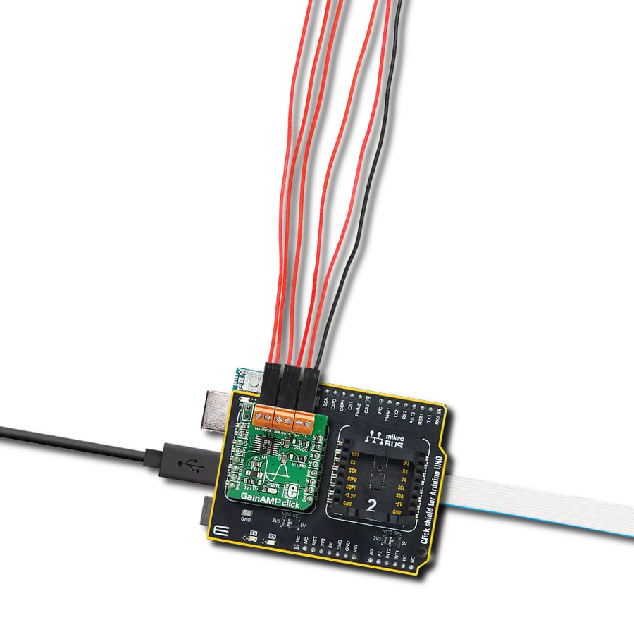
GainAMP Click
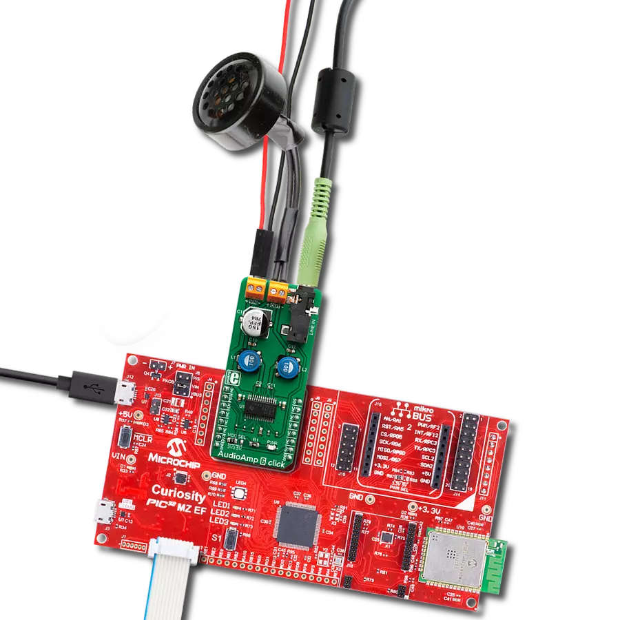
Dev. board
Arduino UNO Rev3
Compiler
NECTO Studio
MCU
ATmega328P
Our PGA solution enables seamless signal amplification with customizable gain settings, making it the ideal choice for your applications where precision and flexibility are paramount
A
A
Hardware Overview
How does it work?
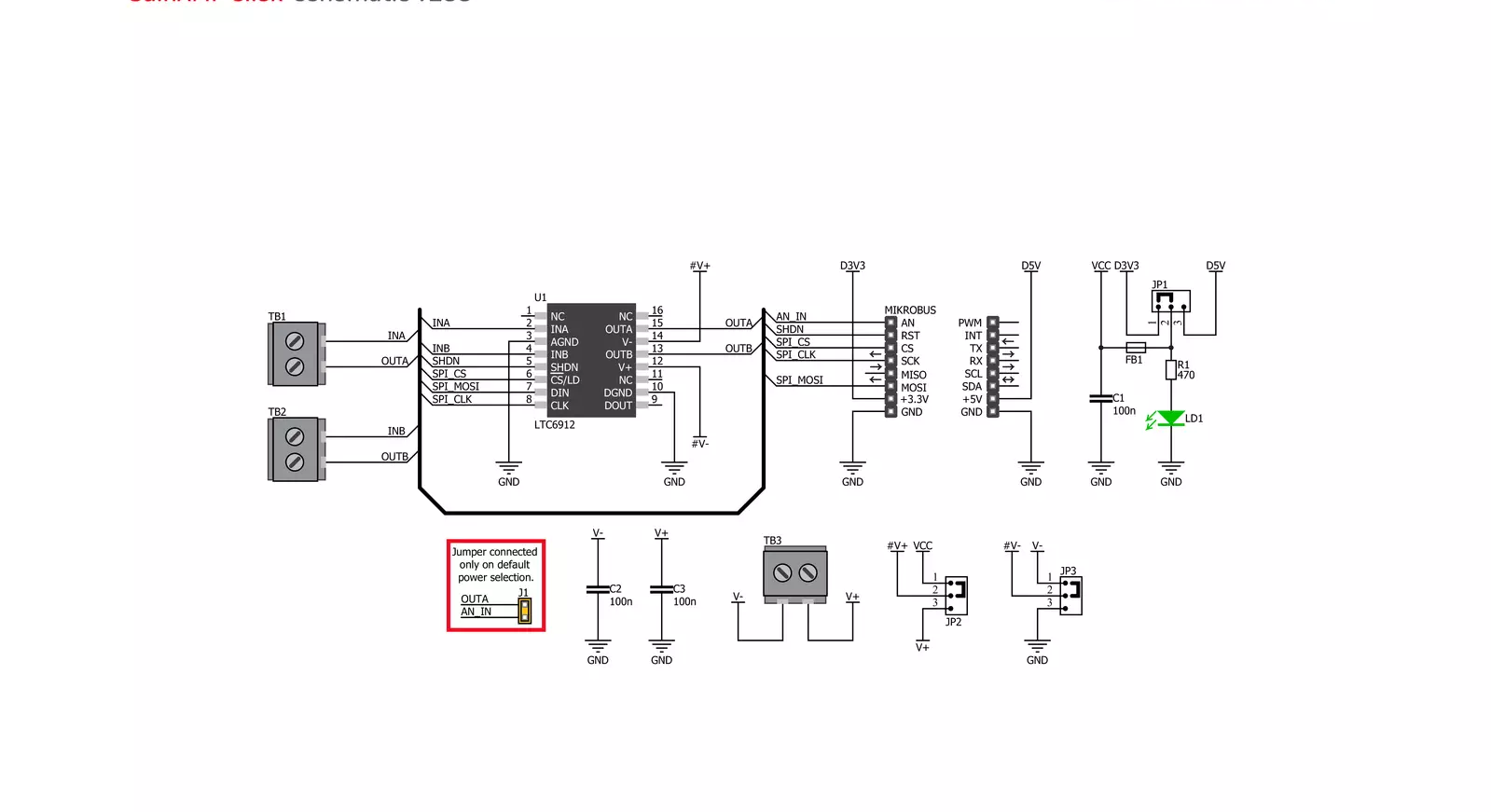
GainAMP Click is based on the LTC6912, a dual channel, low noise, digitally programmable gain amplifier (PGA) from Analog Devices. The click is designed to work on either a 3.3V or 5V power supply. It communicates with the target MCU over the SPI interface, with additional functionality provided by the following pins on the mikroBUS™ line: AN, RST. GainAMP Click also features three
screw terminals and a power indication LED. The gains for both channels are independently programmable, using a 3-wire SPI interface to select voltage gains of 0, 1, 2, 5, 10, 20, 50, and 100V/V (LTC6912-1). All gains are inverting. The LTC6912 consists of 2 matched amplifiers with rail-to-rail outputs. When operated with unity gain, they will also process rail-to-rail input signals.
A half-supply reference generated internally at the AGND pin supports single power supply applications. It operates from single or split supplies from 2.7V to 10.5V in total. A programmable-gain amplifier (PGA) is an electronic amplifier whose gain can be controlled externally (by analog or digital signals).

Features overview
Development board
Arduino UNO is a versatile microcontroller board built around the ATmega328P chip. It offers extensive connectivity options for various projects, featuring 14 digital input/output pins, six of which are PWM-capable, along with six analog inputs. Its core components include a 16MHz ceramic resonator, a USB connection, a power jack, an
ICSP header, and a reset button, providing everything necessary to power and program the board. The Uno is ready to go, whether connected to a computer via USB or powered by an AC-to-DC adapter or battery. As the first USB Arduino board, it serves as the benchmark for the Arduino platform, with "Uno" symbolizing its status as the
first in a series. This name choice, meaning "one" in Italian, commemorates the launch of Arduino Software (IDE) 1.0. Initially introduced alongside version 1.0 of the Arduino Software (IDE), the Uno has since become the foundational model for subsequent Arduino releases, embodying the platform's evolution.

Microcontroller Overview
MCU Card / MCU

Architecture
AVR
MCU Memory (KB)
32
Silicon Vendor
Microchip
Pin count
28
RAM (Bytes)
2048
You complete me!
Accessories
Click Shield for Arduino UNO has two proprietary mikroBUS™ sockets, allowing all the Click board™ devices to be interfaced with the Arduino UNO board without effort. The Arduino Uno, a microcontroller board based on the ATmega328P, provides an affordable and flexible way for users to try out new concepts and build prototypes with the ATmega328P microcontroller from various combinations of performance, power consumption, and features. The Arduino Uno has 14 digital input/output pins (of which six can be used as PWM outputs), six analog inputs, a 16 MHz ceramic resonator (CSTCE16M0V53-R0), a USB connection, a power jack, an ICSP header, and reset button. Most of the ATmega328P microcontroller pins are brought to the IO pins on the left and right edge of the board, which are then connected to two existing mikroBUS™ sockets. This Click Shield also has several switches that perform functions such as selecting the logic levels of analog signals on mikroBUS™ sockets and selecting logic voltage levels of the mikroBUS™ sockets themselves. Besides, the user is offered the possibility of using any Click board™ with the help of existing bidirectional level-shifting voltage translators, regardless of whether the Click board™ operates at a 3.3V or 5V logic voltage level. Once you connect the Arduino UNO board with our Click Shield for Arduino UNO, you can access hundreds of Click boards™, working with 3.3V or 5V logic voltage levels.

Used MCU Pins
mikroBUS™ mapper
Take a closer look
Click board™ Schematic
Step by step
Project assembly

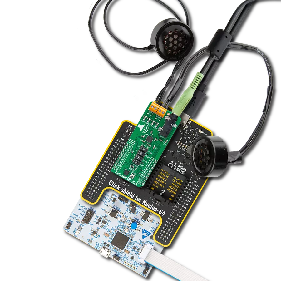
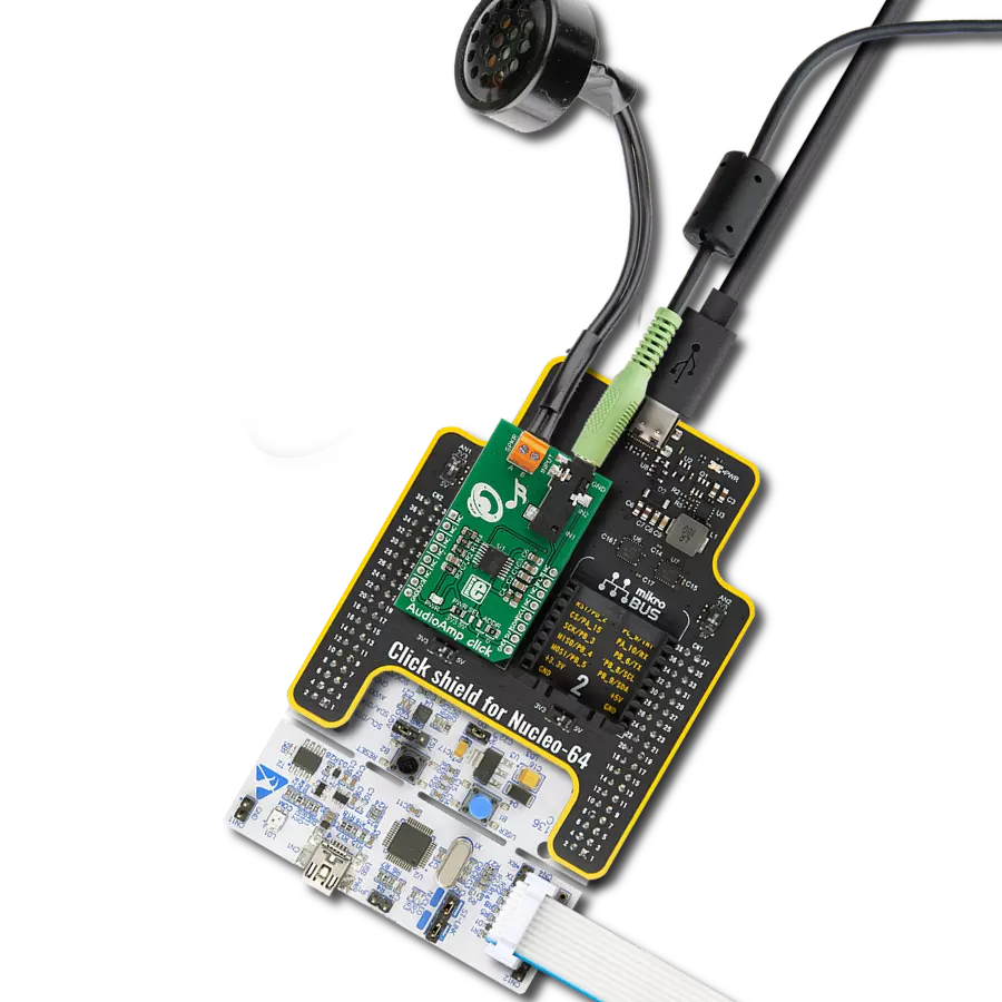
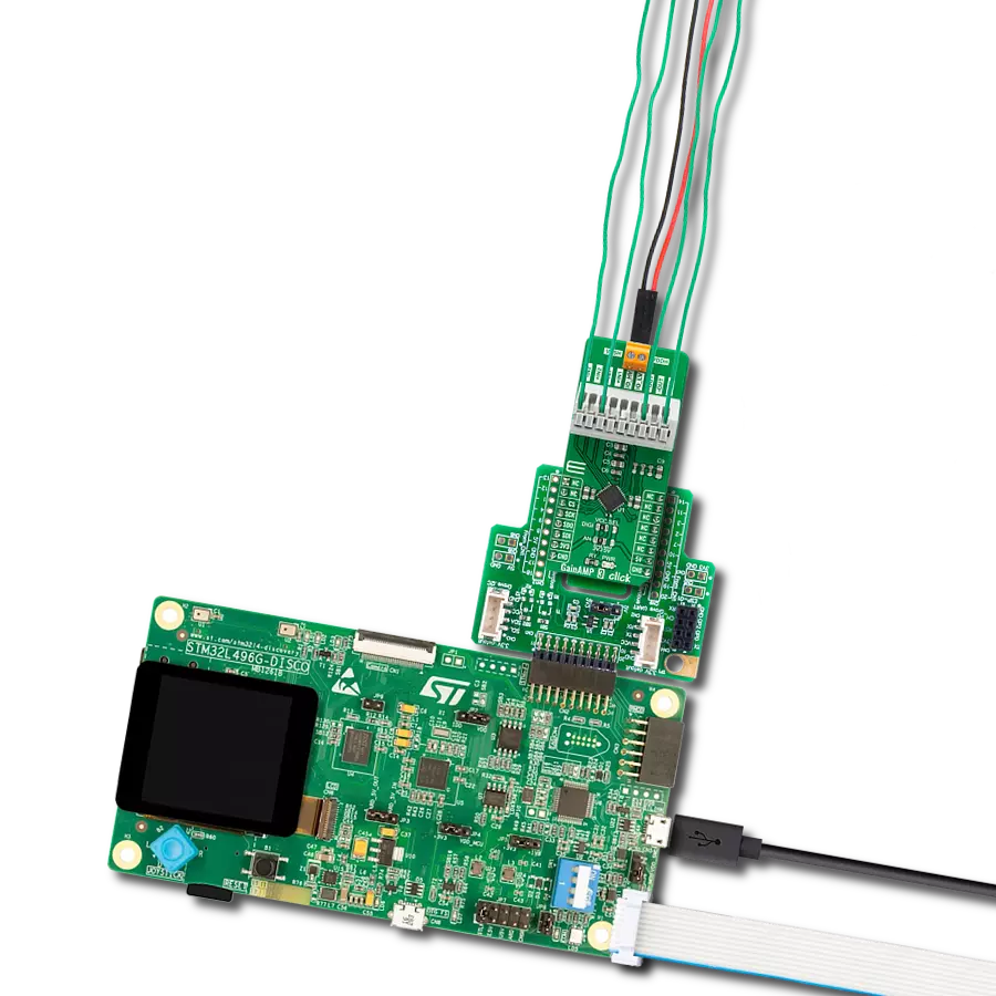
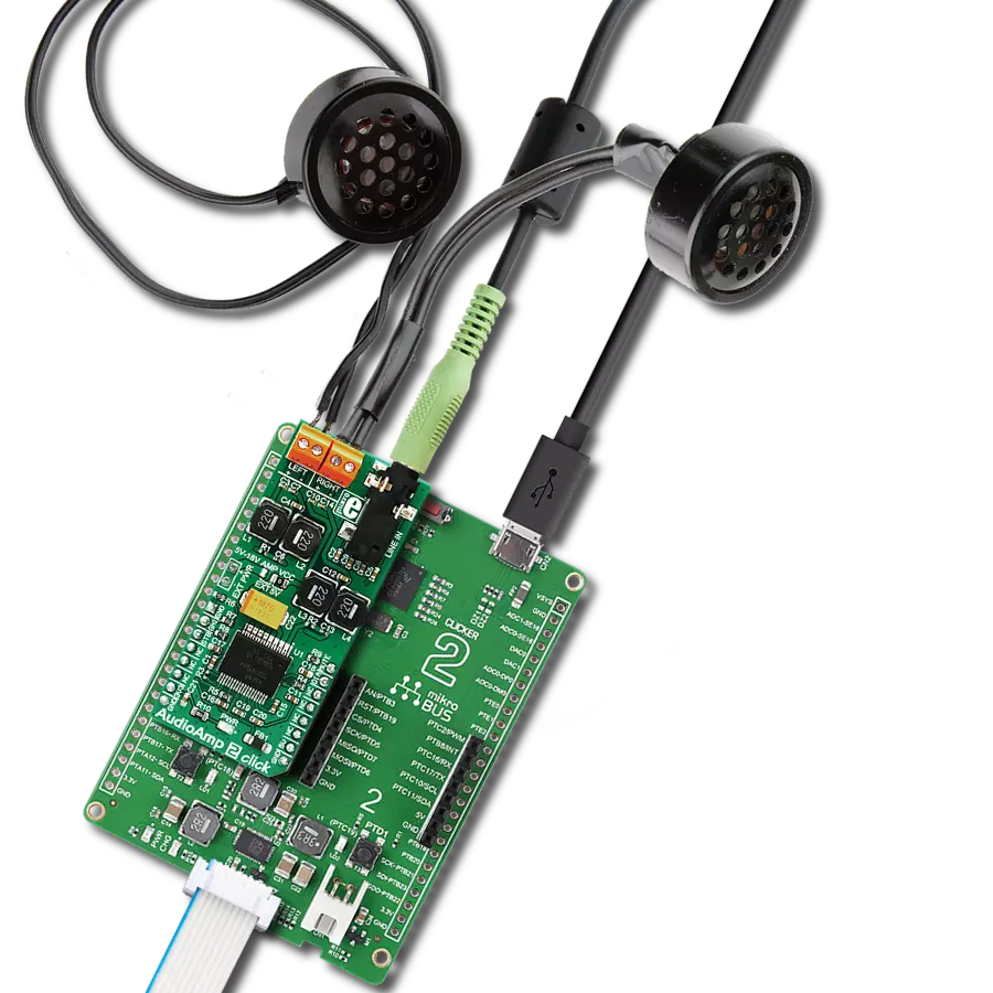
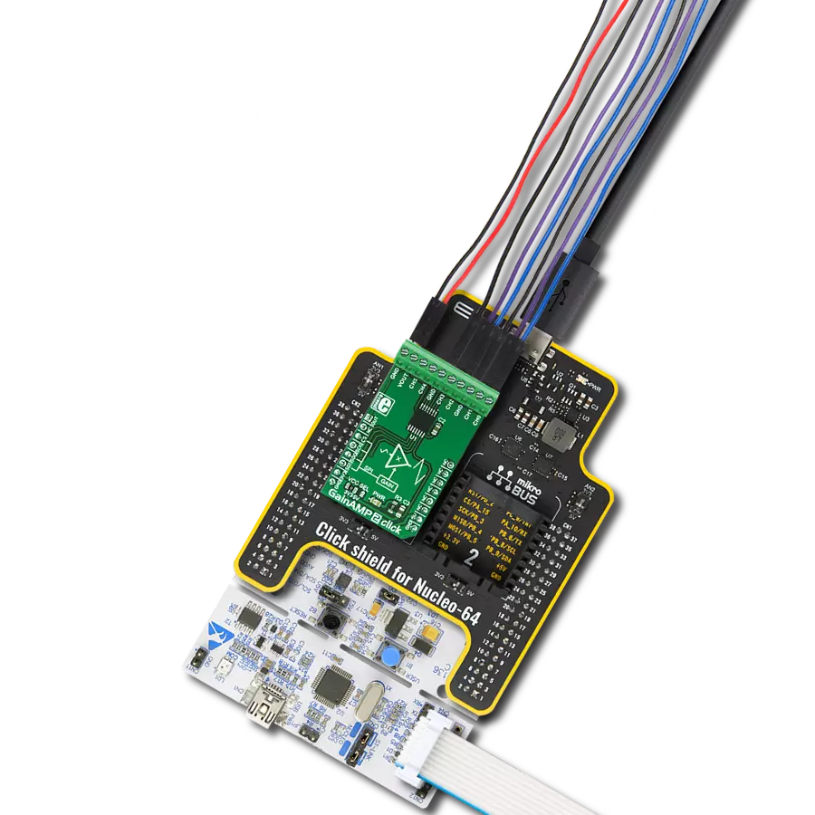
Start by selecting your development board and Click board™. Begin with the Arduino UNO Rev3 as your development board.


Software Support
Library Description
This library contains API for GainAMP Click driver.
Key functions:
gainamp_read_an_pin_value- GainAMP read AN pin value functiongainamp_read_an_pin_voltage- GainAMP read AN pin voltage level functiongainamp_set_gain- Function for sets gain of the GainAMP Click
Open Source
Code example
The complete application code and a ready-to-use project are available through the NECTO Studio Package Manager for direct installation in the NECTO Studio. The application code can also be found on the MIKROE GitHub account.
/*!
 * @file main.c
 * @brief GainAMP Click example
 *
 * # Description
 * This is an example that demonstrates the use of the GainAMP Click board.
 *
 * The demo application is composed of two sections :
 *
 * ## Application Init
 * Initializes SPI module and set CS pin and RST pin as OUTPUT,
 * initialization driver init and resets chip.
 *
 * ## Application Task
 * Sets the gain for both channels, channel A and channel B.
 *
 * @author Stefan Ilic
 *
 */

#include "board.h"
#include "log.h"
#include "gainamp.h"

static gainamp_t gainamp;
static log_t logger;

void application_init ( void )
{
    log_cfg_t log_cfg;  /**< Logger config object. */
    gainamp_cfg_t gainamp_cfg;  /**< Click config object. */

    /**
     * Logger initialization.
     * Default baud rate: 115200
     * Default log level: LOG_LEVEL_DEBUG
     * @note If USB_UART_RX and USB_UART_TX
     * are defined as HAL_PIN_NC, you will
     * need to define them manually for log to work.
     * See @b LOG_MAP_USB_UART macro definition for detailed explanation.
     */
    LOG_MAP_USB_UART( log_cfg );
    log_init( &logger, &log_cfg );
    log_info( &logger, " Application Init " );

    // Click initialization.

    gainamp_cfg_setup( &gainamp_cfg );
    GAINAMP_MAP_MIKROBUS( gainamp_cfg, MIKROBUS_1 );
    err_t init_flag  = gainamp_init( &gainamp, &gainamp_cfg );
    if ( ( SPI_MASTER_ERROR == init_flag ) || ( ADC_ERROR == init_flag ) ) {
        log_error( &logger, " Application Init Error. " );
        log_info( &logger, " Please, run program again... " );

        for ( ; ; );
    }
    gainamp_reset( &gainamp );
    Delay_ms ( 100 );

    log_info( &logger, " Application Task " );
}

void application_task ( void )
{
    gainamp_set_gain( &gainamp, GAINAMP_CHANNEL_A_x1 | GAINAMP_CHANNEL_B_x5 );
    // 10 seconds delay
    Delay_ms ( 1000 );
    Delay_ms ( 1000 );
    Delay_ms ( 1000 );
    Delay_ms ( 1000 );
    Delay_ms ( 1000 );
    Delay_ms ( 1000 );
    Delay_ms ( 1000 );
    Delay_ms ( 1000 );
    Delay_ms ( 1000 );
    Delay_ms ( 1000 );

    gainamp_set_gain( &gainamp, GAINAMP_CHANNEL_A_x10 | GAINAMP_CHANNEL_B_x100 );
    // 10 seconds delay
    Delay_ms ( 1000 );
    Delay_ms ( 1000 );
    Delay_ms ( 1000 );
    Delay_ms ( 1000 );
    Delay_ms ( 1000 );
    Delay_ms ( 1000 );
    Delay_ms ( 1000 );
    Delay_ms ( 1000 );
    Delay_ms ( 1000 );
    Delay_ms ( 1000 );
}

int main ( void )
{
    /* Do not remove this line or clock might not be set correctly. */
    #ifdef PREINIT_SUPPORTED
    preinit();
    #endif

    application_init( );

    for ( ; ; )
    {
        application_task( );
    }

    return 0;
}

// ------------------------------------------------------------------------ END
Additional Support
Resources
Category:Amplifier