Simplify data representation with a 10-segment bar graph based on XGURUGX10D and STM32F302VC
Graph-tastic voyage: Sailing through data in style!
Published Jul 22, 2025
Click board™
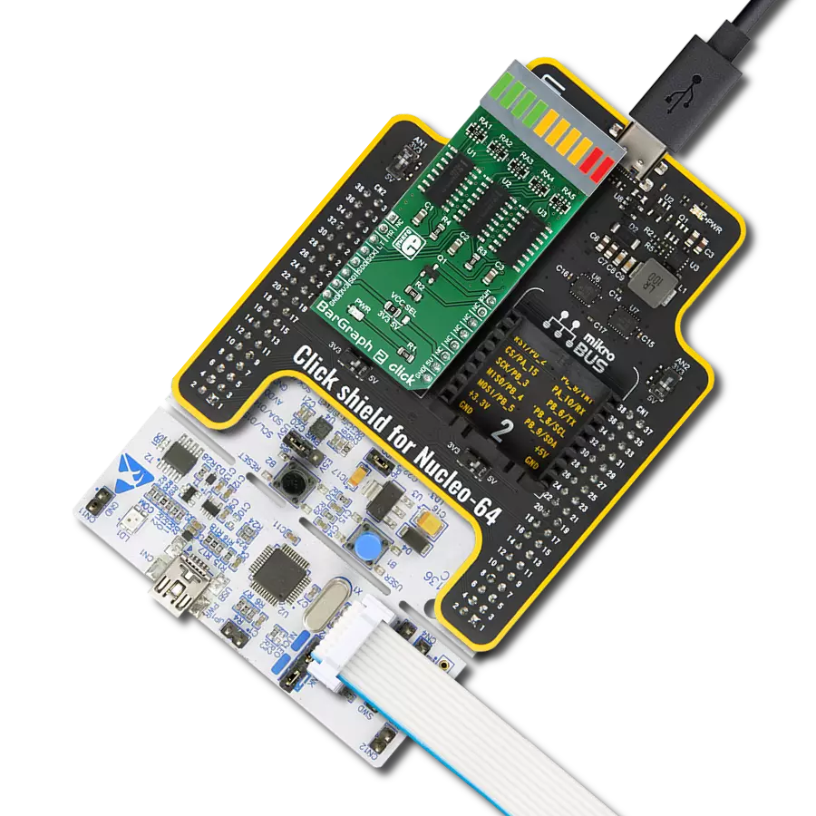
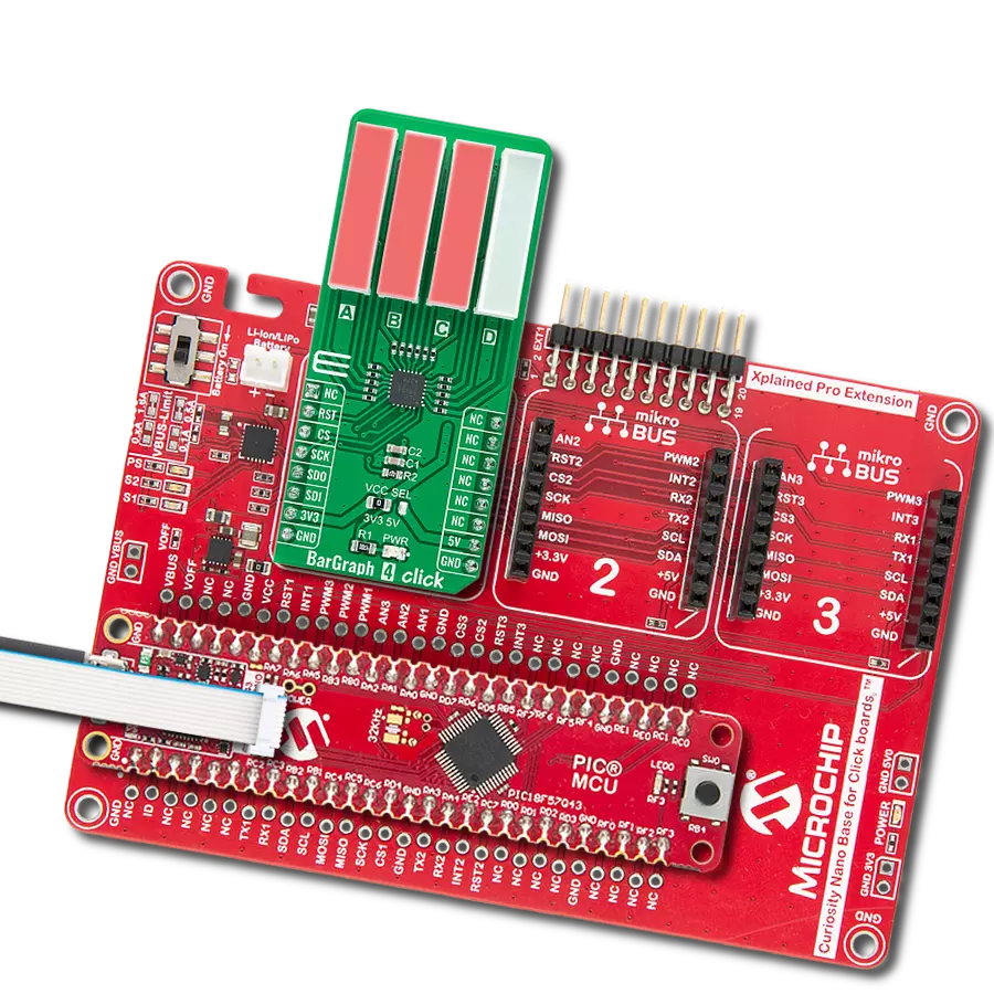
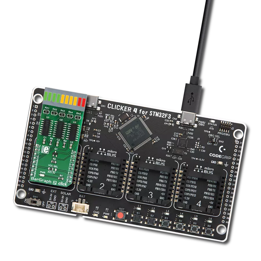
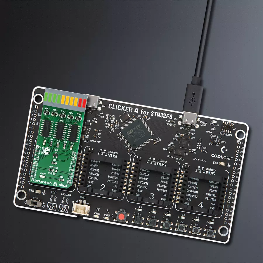
BarGraph 2 Click
Dev. board
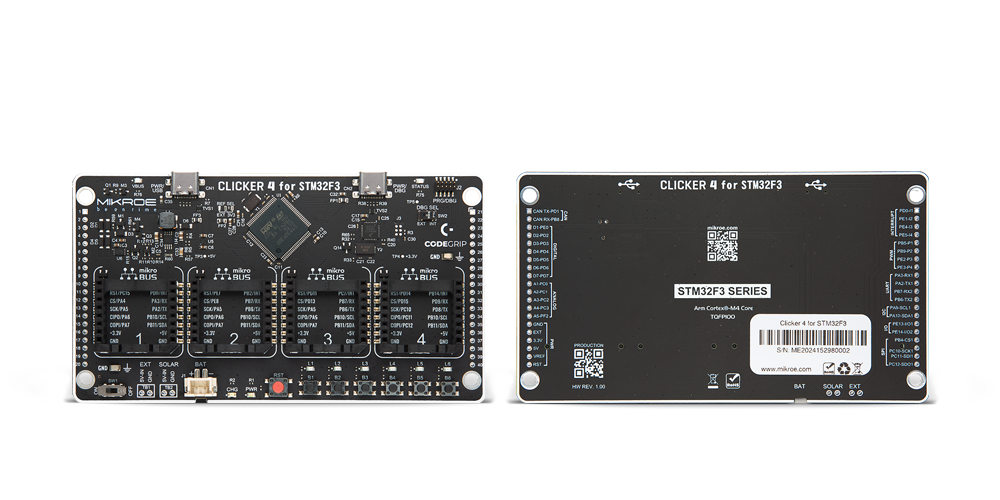
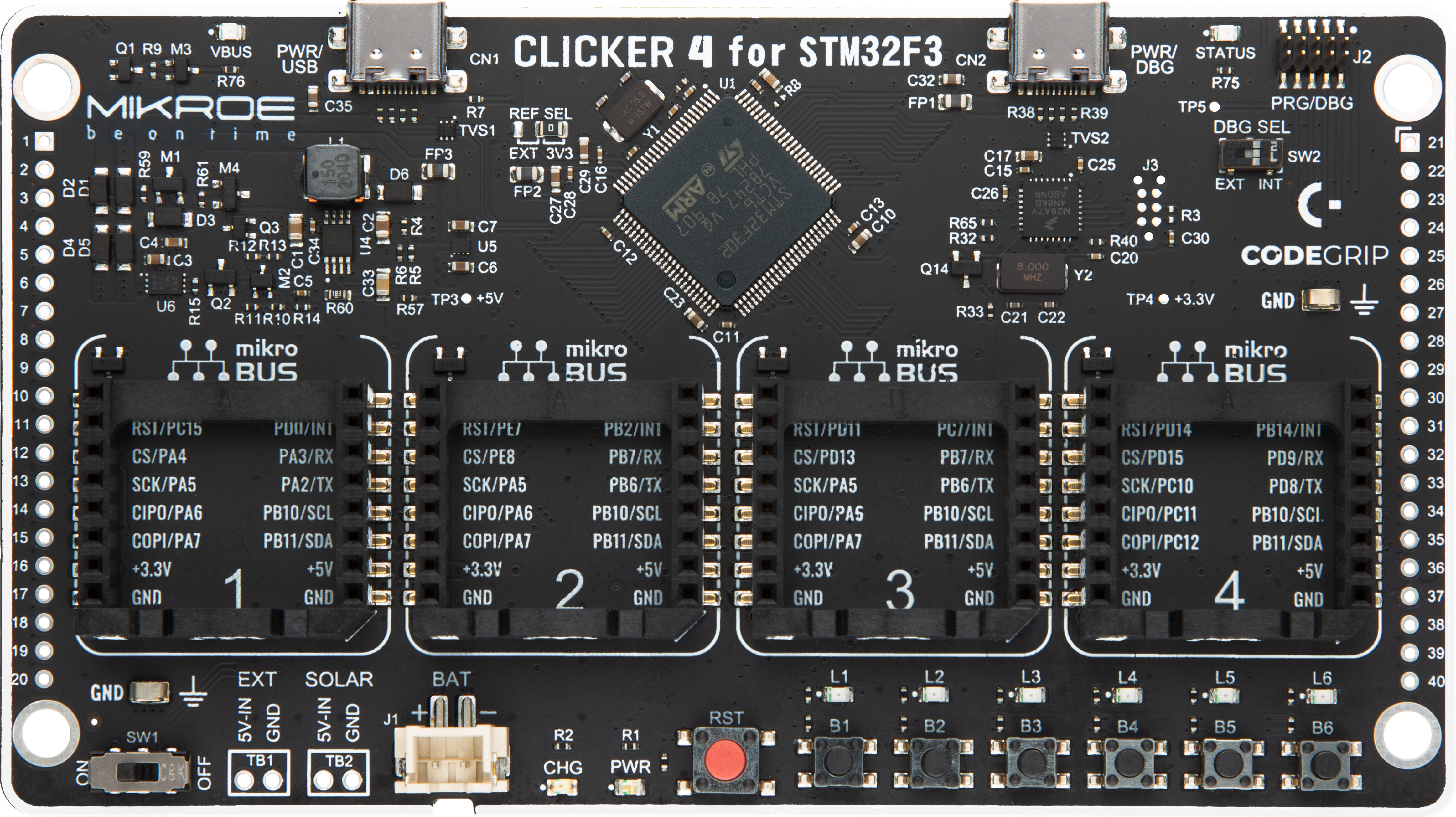
CLICKER 4 for STM32F302VCT6
Compiler
NECTO Studio
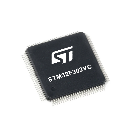
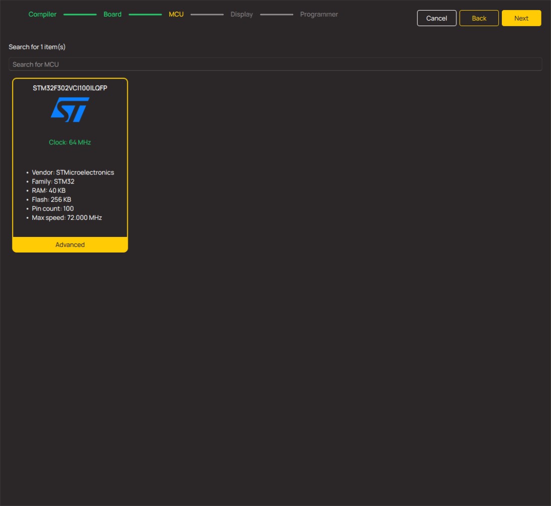
MCU
STM32F302VC
Our 10-segment bar graph display solution is the epitome of data elegance, designed to provide individuals with a sophisticated and precise tool for visualizing data insights
A
A
Hardware Overview
How does it work?
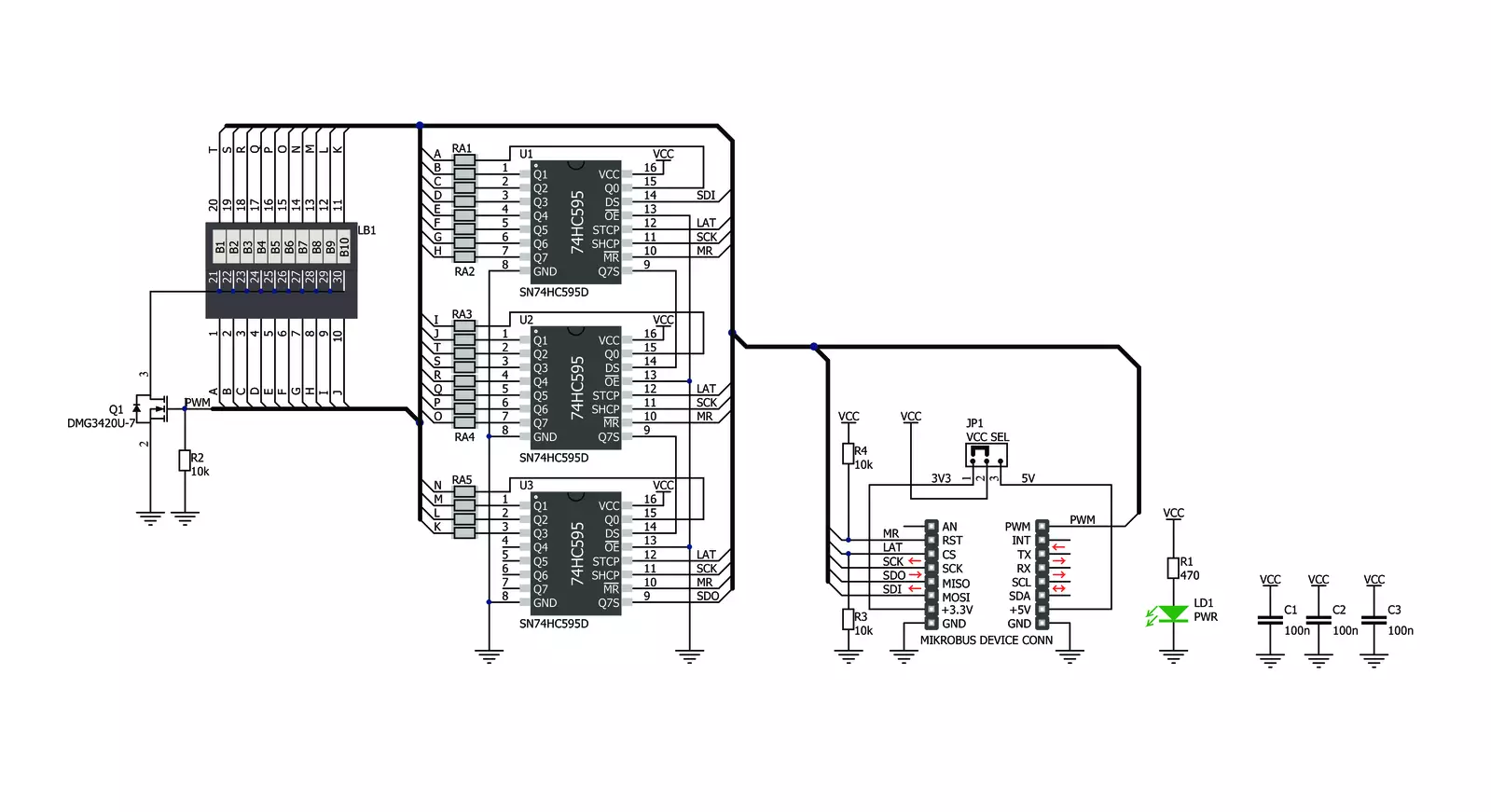
BarGraph 2 Click is based on three 74HC595, 8-bit serial-in, parallel-out shift registers with output latches from Texas Instruments to drive the XGURUGX10D, a 10-segment bar graph array, from SunLED. The 74HC595 ICs are comprised of a D-type internal storage register and the serial-to-parallel shift register, both 8-bit wide. Each of these registers has its own clock line, making it possible to clock in the desired data and then clock it out to the parallel output pins. The XGURUGX10D bar graph LED array has 10 dual-color segments. Each segment contains red and green LED, thus having two anodes and one cathode per segment. This results in having 20 LED anodes and 10 LED cathodes, in total. The XGURUGX10D bar graph display is connected as a common cathode type display, meaning that all LED cathodes are routed to a single point. The LED cathode line is connected to the drain of the N channel MOSFET, while its source is connected to the GND. Driving this MOSFET via its gate through the PWM pin of the mikroBUS™ allows dimming of the LED segments. By changing the duty cycle of the PWM signal, it is possible to change the brightness of the XGURUGX10D bar graph display. The Click board™ communicates
with the host MCU via the SPI interface, routed to the mikroBUS™ MOSI, MISO and SCK pins, labeled as SDI, SDO and SCK on this Click board™, respectively. Three bytes of information (24 bits in total) are pushed through the serial data input pin (DS) of the first 74HC595 IC, routed to the SDI pin. The 74HC595 construction is such that after receiving 8 bits, clocking in one more bit will shift the existing 8 bits by one place, overflowing the last bit to the Q7S output pin, shifting it out that way. Since the Q7S of the first 74HC595 is connected to the DS pin of the second 74HC595 (and the Q7S of the second IC is connected to the DS pin of the third 74HC595 IC), clocking in 24 bits to the first 74HC595 IC will fill up all three ICs. It is worth mentioning that the Q7S of the last 74HC595 IC is routed to the MISO pin of the mikroBUS™, labeled as the SDO, allowing connection of multiple devices in cascade, building more complex setups. Adding more devices in cascade would require more 8bit words to be clocked in the first 74HC595 IC. The first 10 bits are used to control all the green LEDs of the segments. The second 10 bits are used to control all the red LEDs of the segments. Since the MCU usually clocks out no less than 8 bits through the
SPI per cycle, the last 4 bits of the total of 24 bits, are disregarded. When the data has been clocked in, the SPI clock should stop and the CS pin should be driven to a HIGH logic level. The CS pin of the mikroBUS™ is routed to the STCP pin of the 74HC595 ICs, and it is labeled as LT. A rising edge on the STCP input pins of the 74HC595 ICs will latch the data from their internal storage registers to the output pins, polarizing the connected bar graph segment anodes. The STCP pin is pulled to a LOW logic level by the onboard resistor. The #MR pin is used to clear the data in the internal storage register of the ICs. The LOW logic level on this pin will clear the content of this storage register, but it will not turn off the outputs which are already activated. The #MR pin is routed to the RST pin of the mikroBUS™, labeled as MR and it is pulled to a HIGH logic level by the onboard resistor. This Click board™ can operate with either 3.3V or 5V logic voltage levels selected via the VCC SEL jumper. This way, both 3.3V and 5V capable MCUs can use the communication lines properly. Also, this Click board™ comes equipped with a library containing easy-to-use functions and an example code that can be used as a reference for further development.


Features overview
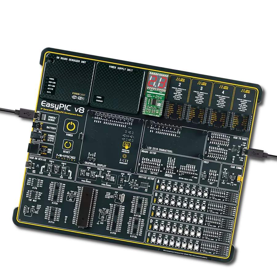
Development board
Clicker 4 for STM32F3 is a compact development board designed as a complete solution, you can use it to quickly build your own gadgets with unique functionalities. Featuring a STM32F302VCT6, four mikroBUS™ sockets for Click boards™ connectivity, power managment, and more, it represents a perfect solution for the rapid development of many different types of applications. At its core, there is a STM32F302VCT6 MCU, a powerful microcontroller by STMicroelectronics, based on the high-
performance Arm® Cortex®-M4 32-bit processor core operating at up to 168 MHz frequency. It provides sufficient processing power for the most demanding tasks, allowing Clicker 4 to adapt to any specific application requirements. Besides two 1x20 pin headers, four improved mikroBUS™ sockets represent the most distinctive connectivity feature, allowing access to a huge base of Click boards™, growing on a daily basis. Each section of Clicker 4 is clearly marked, offering an intuitive and clean interface. This makes working with the development
board much simpler and thus, faster. The usability of Clicker 4 doesn’t end with its ability to accelerate the prototyping and application development stages: it is designed as a complete solution which can be implemented directly into any project, with no additional hardware modifications required. Four mounting holes [4.2mm/0.165”] at all four corners allow simple installation by using mounting screws. For most applications, a nice stylish casing is all that is needed to turn the Clicker 4 development board into a fully functional, custom design.
Microcontroller Overview
MCU Card / MCU
Architecture
ARM Cortex-M4
MCU Memory (KB)
256
Silicon Vendor
STMicroelectronics
Pin count
100
RAM (Bytes)
40960
Used MCU Pins
mikroBUS™ mapper
Take a closer look
Click board™ Schematic
Step by step
Project assembly
Start by selecting your development board and Click board™. Begin with the CLICKER 4 for STM32F302VCT6 as your development board.


Software Support
Library Description
This library contains API for BarGraph 2 Click driver.
Key functions:
bargraph2_led_green- This function turns on the green LED diode of the chosen segmentbargraph2_leds_green- This function turns on green LED diodes from the starting index to the end indexbargraph2_lights_out- This function turns off all the LED diodes.
Open Source
Code example
The complete application code and a ready-to-use project are available through the NECTO Studio Package Manager for direct installation in the NECTO Studio. The application code can also be found on the MIKROE GitHub account.
/*!
 * \file
 * \brief Bargraph2 Click example
 *
 * # Description
 * The example starts off with the initalisation and configuration of the logger and Click
 * modules and later on showcases different ways of lighting LED diodes on the Click.
 *
 * The demo application is composed of two sections :
 *
 * ## Application Init
 * This function initializes and configures the logger and Click modules.
 *
 * ## Application Task
 * This function shows the user how to light single and multiple LED diodes.
 *
 * \author MikroE Team
 *
 */
// ------------------------------------------------------------------- INCLUDES

#include "board.h"
#include "log.h"
#include "bargraph2.h"

// ------------------------------------------------------------------ VARIABLES

static bargraph2_t bargraph2;
static log_t logger;

// ------------------------------------------------------ APPLICATION FUNCTIONS

void application_init ( )
{
    log_cfg_t log_cfg;
    bargraph2_cfg_t cfg;

    /**
     * Logger initialization.
     * Default baud rate: 115200
     * Default log level: LOG_LEVEL_DEBUG
     * @note If USB_UART_RX and USB_UART_TX
     * are defined as HAL_PIN_NC, you will
     * need to define them manually for log to work.
     * See @b LOG_MAP_USB_UART macro definition for detailed explanation.
     */
    LOG_MAP_USB_UART( log_cfg );
    log_init( &logger, &log_cfg );
    log_info( &logger, "---- Application Init ----" );

    //  Click initialization.

    bargraph2_cfg_setup( &cfg );
    BARGRAPH2_MAP_MIKROBUS( cfg, MIKROBUS_1 );
    bargraph2_init( &bargraph2, &cfg );

    barpgraph2_power( &bargraph2, BARGRAPH2_POWER_ON );
}

void application_task ( )
{
    uint8_t cnt;

    // Single LED switch

    for ( cnt = 1; cnt <= 10; cnt++ )
    {
        bargraph2_led_green( &bargraph2, cnt );
        Delay_ms ( 200 );
        bargraph2_led_red( &bargraph2, 10 - ( cnt - 1 ) );
        Delay_ms ( 200 );
    }

    bargraph2_lights_out ( &bargraph2 );

    // Multiple LED switch

    bargraph2_leds_green ( &bargraph2, 1, 10 );
    Delay_ms ( 1000 );
    bargraph2_leds_red ( &bargraph2, 1, 10 );
    Delay_ms ( 1000 );
    bargraph2_leds_yellow ( &bargraph2, 1, 10 );
    Delay_ms ( 1000 );
}

int main ( void )
{
    /* Do not remove this line or clock might not be set correctly. */
    #ifdef PREINIT_SUPPORTED
    preinit();
    #endif

    application_init( );

    for ( ; ; )
    {
        application_task( );
    }

    return 0;
}

// ------------------------------------------------------------------------ END
Additional Support
Resources
Category:LED Segment